BA00CC0WFPWT-V5
Description
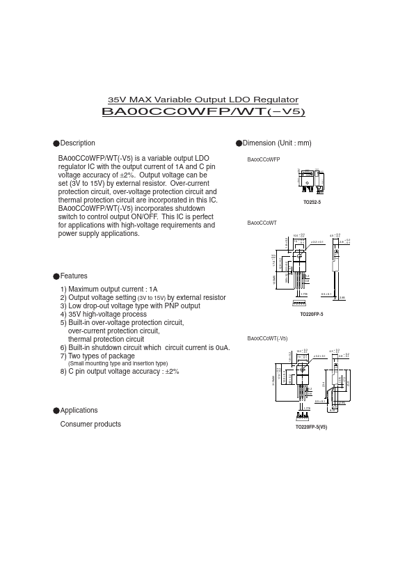
BA00CC0WFP/WT(-V5) is a variable output LDO regulator IC with the output current of 1A and C pin voltage accuracy of ±2%.
BA00CC0WFP/WT(-V5) is a variable output LDO regulator IC with the output current of 1A and C pin voltage accuracy of ±2%.