Part number:
RU30L30M3
Manufacturer:
Ruichips
File Size:
366.41 KB
Description:
P-channel advanced power mosfet.
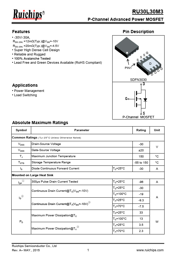
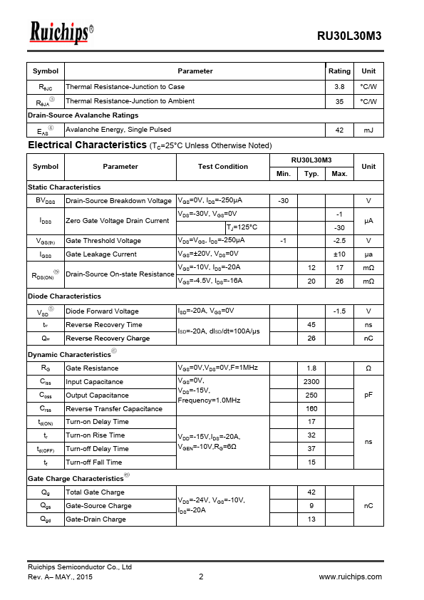
RU30L30M3 Features
* -30V/-30A, RDS (ON) =12mΩ(Typ.)@VGS=-10V RDS (ON) =20mΩ(Typ.)@VGS=-4.5V
* Super High Dense Cell Design
* Reliable and Rugged
* 100% Avalanche Tested
* Lead Free and Green Devices Available (RoHS Compliant) Applications
* Power Management
* Lo
RU30L30M3 Datasheet (366.41 KB)
Datasheet Details
RU30L30M3
Ruichips
366.41 KB
P-channel advanced power mosfet.
📁 Related Datasheet
RU30L30M P-Channel Advanced Power MOSFET (Ruichips)
RU30L15H P-Channel Advanced Power MOSFET (Ruichips)
RU30 Fast-Recovery Rectifier Diodes (Sanken electric)
RU30100L N-Channel Advanced Power MOSFET (Ruichips)
RU30100R N-Channel Advanced Power MOSFET (Ruichips)
RU30105L N-Channel Advanced Power MOSFET (Ruichips)
RU30105R N-Channel Advanced Power MOSFET (Ruichips)
RU30106L N-Channel Advanced Power MOSFET (Ruichips)
RU30L30M3 Distributor