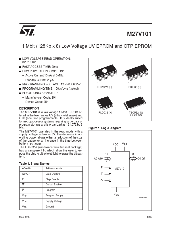
M27V101
Key Features
- Read Mode DC Characteristics (1) (TA = 0 to 70°C or -40 to 85°C; VCC = 3.3V ± 10%; VPP = VCC) Symbol ILI ILO ICC ICC1 ICC2 IPP VIL VIH (2) VOL VOH Parameter Input Leakage Current Output Leakage Current Supply Current Supply Current (Standby) TTL Supply Current (Standby) CMOS Program Current Input Low Voltage Input High Voltage Output Low Voltage Output High Voltage TTL Output High Voltage CMOS IOL = 2.1mA IOH = -400µA IOH = -100µA 2.4 Vcc - 0.7V Test Condition 0V ≤ VIN ≤ V CC 0V ≤ VOUT ≤ VCC E = VIL, G = VIL, IOUT = 0mA, f = 5MHz, V CC ≤ 3.6V E = VIH E > VCC - 0.2V, VCC ≤ 3.6V VPP = VCC -0.3 2 Min Max ± 10 ± 10 15 1 20 10 0.8 VCC + 1 0.4 Unit µA µA mA mA µA µA V V V V V Note:
- VCC must be applied simultaneously with or before VPP and removed simultaneously or after V PP.
- Maximum DC voltage on Output is VCC +0.5V. Table 8A. Read Mode AC Characteristics (1) (TA = 0 to 70 °C or -40 to 85°; VCC = 3.3V ± 10%; VPP = VCC) M27V101 Symbol Alt Parameter Test Condition - 90 (3) Min tAVQV tELQV tGLQV tEHQZ (2) tGHQZ (2) tAXQX tACC tCE tOE tDF tDF tOH Address Valid to Output Valid Chip Enable Low to Output Valid Output Enable Low to Output Valid Chip Enable High to Output Hi-Z Output Enable High to Output Hi-Z Address Transition to Output Transition E = VIL, G = VIL G = VIL E = VIL G = VIL E = VIL E = VIL, G = VIL 0 0 0 Max 90 90 45 30 30 0 0 0 -100 Min Max 100 100 50 30 30 ns ns ns ns ns ns Unit Note:
- Sampled only, not 100% tested.
- Speed obtained with High Speed AC measurament conditions. The associated transient voltage peaks can be suppressed by complying with the two line output control and by properly selected decoupling capacitors. It is recommended that a 0.1µF ceramic capacitor be used on every device between VCC and VSS. This should be a high frequency capacitor of low inherent inductance and should be placed as close to the device as possible. In addition, a 4.7µF bulk electrolytic capacitor should be used between VCC and VSS for every eight devices. The bulk capacitor should be located near the power supply connection point. The purpose of the bulk capacitor is to overcome the voltage drop caused by the inductive effects of PCB traces. 5/15 M27V101 Table 8B. Read Mode AC Characteristics (1) (TA = 0 to 70° C or -40 to 85 °C; VCC = 3.3V ± 10%; VPP = Vcc) M27V201 Symbol Alt Parameter Test Conditi on -120 Min tAVQV tELQV tGLQV tEHQZ (2) tGHQZ (2) tAXQX tACC tCE tOE tDF tDF tOH Address Valid to Output Valid Chip Enable Low to Output Valid Output Enable Low to Output Valid Chip Enable High to Output Hi-Z Output Enable High to Output Hi-Z Address Transition to Output Transition E = VIL, G = VIL G = VIL