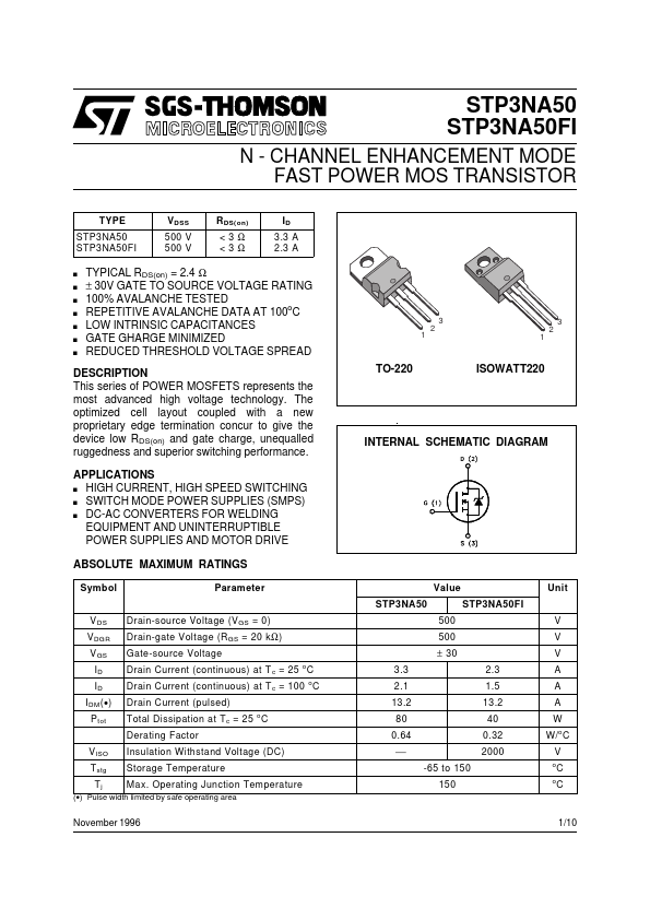
Datasheet4U Logo Datasheet4U.com

P3NA50 Datasheet STP3NA50

Manufacturer: STMicroelectronics

General Description

This series of POWER MOSFETS represents the most advanced high voltage technology.

The optimized cell layout coupled with a new proprietary edge termination concur to give the device low RDS(on) and gate charge, unequalled ruggedness and superior switching performance.

APPLICATIONS s HIGH CURRENT, HIGH SPEED SWITCHING s SWITCH MODE POWER SUPPLIES (SMPS) s DC-AC CONVERTERS FOR WELDING EQUIPMENT AND UNINTERRUPTIBLE POWER SUPPLIES AND MOTOR DRIVE ABSOLUTE MAXIMUM RATINGS Symbol Parameter VDS Drain-source Voltage (VGS = 0) VDGR Drain-gate Voltage (RGS = 20 kΩ) VGS Gate-source Voltage ID Drain Current (continuous) at Tc = 25 oC ID Drain Current (continuous) at Tc = 100 oC IDM(•) Drain Current (pulsed) Ptot Total Dissipation at Tc = 25 oC Derating Factor VISO Insulation Withstand Voltage (DC) Tstg Storage Temperature Tj Max.

Overview

STP3NA50 STP3NA50FI N - CHANNEL ENHANCEMENT MODE FAST POWER MOS TRANSISTOR TYPE STP3NA50 STP3NA50FI VDSS 500 V 500 V RDS(on) <3Ω <3Ω ID 3.3 A 2.3 A s TYPICAL RDS(on) = 2.