Datasheet Summary
..
STP7NB60 STP7NB60FP
- CHANNEL ENHANCEMENT MODE PowerMESH™ MOSFET
TYPE STP7NB60 STP7NB60F P s s s s s
V DSS 600 V 600 V
R DS(on) < 1.2 Ω < 1.2 Ω
ID 7.2 A 4.1 A
TYPICAL RDS(on) = 1.0 Ω EXTREMELY HIGH dv/dt CAPABILITY 100% AVALANCHE TESTED VERY LOW INTRINSIC CAPACITANCES GATE CHARGE MINIMIZED
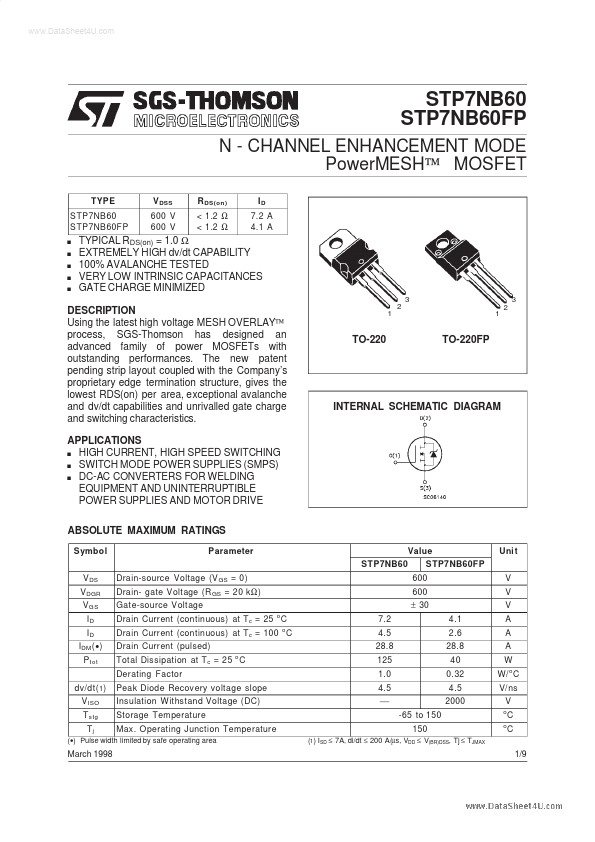
1 2 3
1 2 3
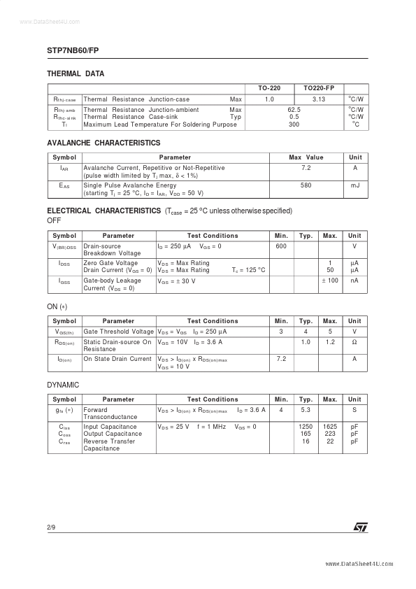
DESCRIPTION Using the latest high voltage MESH OVERLAY™ process, SGS-Thomson has designed an advanced family of power MOSFETs with outstanding performances. The new patent pending strip layout coupled with the pany’s proprietary edge termination structure, gives the lowest RDS(on) per area, exceptional avalanche and dv/dt capabilities and unrivalled gate charge...