Datasheet4U Logo Datasheet4U.com

STF9NK60ZD Datasheet N-channel Power MOSFET

Manufacturer: STMicroelectronics

Overview: STP9NK60ZD - STF9NK60ZD STB9NK60ZD N-CHANNEL 600V - 0.85Ω - 7A TO-220/TO-220FP/D2PAK SuperFREDMesh™ MOSFET ADVANCED DATA TYPE STP9NK60ZD STF9NK60ZD STB9NK60ZD s VDSS 600 V 600 V 600 V RDS(on) < 0.95 Ω < 0.95 Ω < 0.95 Ω ID 7A 7A 7A Pw 125 W 30 W 125 W 3 1 2 TYPICAL RDS(on) = 0.85 Ω s VERY HIGH dv/dt CAPABILITY s 100% AVALANCHE TESTED www.DataSheet4U.

General Description

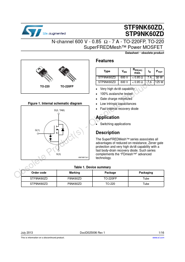
The SuperFREDMesh™ series associates all advantages of reduced on-resistance, zener gate protection and very high dv/dt capability with a Fast body-drain recovery diode.

Such series complements the “FDmesh™” Advanced Technology.

APPLICATIONS s HID BALLAST s ZVS PHASE-SHIFT FULL BRIDGE CONVERTERS D2PAK INTERNAL SCHEMATIC DIAGRAM ORDERING INFORMATION SALES TYPE STP9NK60ZD STF9NK60ZD STB9NK60ZDT4 MARKING P9NK60ZD F9NK60ZD B9NK60ZD PACKAGE TO-220 TO-220FP D PAK 2 PACKAGING TUBE TUBE TAPE & REEL January 2004 1/12 STP9NK60ZD - STF9NK60ZD - STB9NK60ZD ABSOLUTE MAXIMUM RATINGS Symbol Parameter Value TO-220 / D2PAK VDS VDGR VGS ID ID IDM ( ) PTOT VESD(G-S) Drain-source Voltage (VGS = 0) Drain-gate Voltage (RGS = 20 kΩ) Gate- source Voltage Drain Current (continuos) at TC = 25°C Drain Current (continuos) at TC = 100°C Drain Current (pulsed) Total Dissipation at TC = 25°C Derating Factor Gate source ESD (HBM-C=100pF, R=1.5KΩ) Peak Diode Recovery voltage slope Insulation Withstand Voltage (DC) Operating Junction Temperature Storage Temperature -55 to 150 dv/dt (1) VISO Tj Tstg 7 4.3 28 125 1 4000 15 2500 600 600 ± 30 7 (*) 4.3 (*) 28 (*) 30 0.24 TO-220FP V V V A A A W W/°C V V/ns V °C Unit www.DataSheet4U.com ( ) Pulse width limited by safe operating area (1) ISD ≤7A, di/dt ≤500A/µs, VDD ≤ V(BR)DSS, Tj = 25°C (*) Limited only by maximum temperature allowed THERMAL DATA TO-220 D2PAK Rthj-pcb Rthj-case Rthj-amb Tl Thermal Resistance Junction-pcb Max (When mounted on minimum Footprint) TO-220FP Uni

Key Features

  • OF GATE-TO-SOURCE ZENER DIODES The built-in back-to-back Zener diodes have specifically been designed to enhance not only the device’s ESD capability, but also to make them safely absorb possible voltage transients that may occasionally be applied from gate to souce. In this respect the Zener voltage is appropriate to achieve an efficient and costeffective intervention to protect the device’s integrity. These integrated Zener diodes thus avoid the usage of external components. 2/12 STP9NK60ZD.

STF9NK60ZD Distributor & Price

Compare STF9NK60ZD distributor prices and check real-time stock availability from major suppliers. Prices and inventory may vary by region and order quantity.