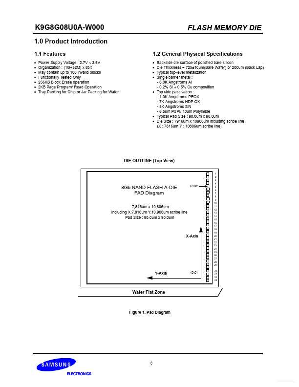
K9G8G08U0A-W000 Key Features
- Power Supply Voltage : 2.7V ~ 3.6V Organization : (1G+32M) x 8bit May contain up to 100 invalid blocks Functionally Test
- Backside die surface of polished bare silicon Die Thickness = 725±10um(Bare Wafer) or 200um (Back Lap) Typical top-level
- 6.0K Angstroms Al
- 0.2% Si + 0.5% Cu position
- Top side passivation
- 1.0K Angstroms PEOX
- 7K Angstroms HDP OX
- 3K Angstroms SiN
- 6.5um PSPI/ 10um Polyimide
- Typical Pad Size : 90.0um x 90.0um