K7P321888M Description
K7P323688M K7P321888M 1Mx36 & 2Mx18 SRAM .. 32Mb M-die LW SRAM Specification 119BGA with Pb & Pb-Free (RoHS pliant) INFORMATION IN THIS DOCUMENT IS PROVIDED IN RELATION TO SAMSUNG PRODUCTS, AND IS SUBJECT TO CHANGE WITHOUT NOTICE. NOTHING IN THIS DOCUMENT SHALL BE CONSTRUED AS GRANTING ANY LICENSE, EXPRESS OR IMPLIED, BY ESTOPPEL OR OTHERWISE, TO ANY INTELLECTUAL PROPERTY RIGHTS IN SAMSUNG PRODUCTS OR TECHNOLOGY.
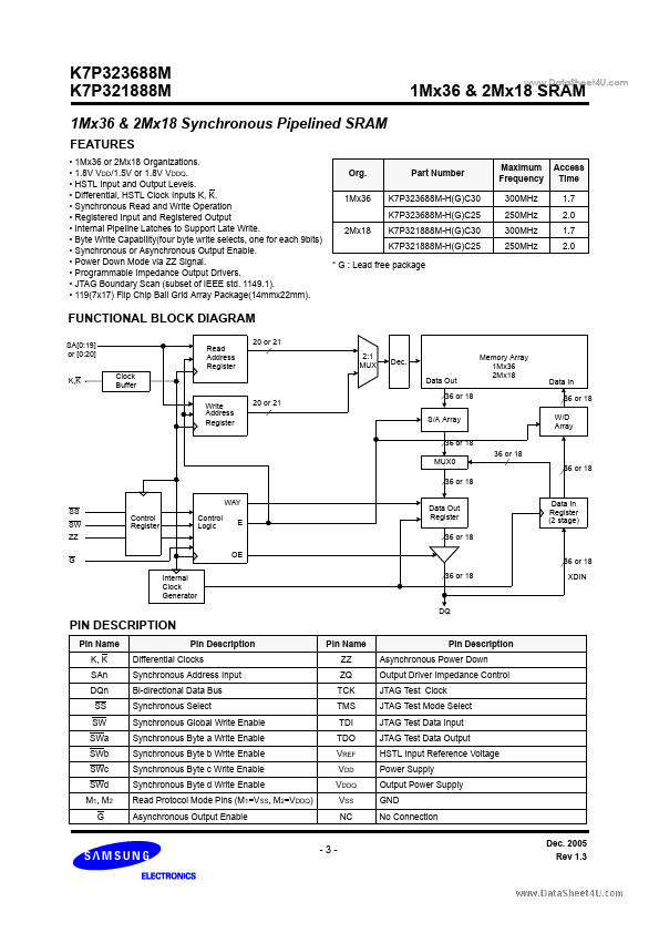
K7P321888M Key Features
- 1Mx36 or 2Mx18 Organizations
- 1.8V VDD/1.5V or 1.8V VDDQ
- HSTL Input and Output Levels
- Differential, HSTL Clock Inputs K, K
- Synchronous Read and Write Operation
- Registered Input and Registered Output
- Internal Pipeline Latches to Support Late Write
- Byte Write Capability(four byte write selects, one for e
K7P321888M Applications
- Samsung Electronics reserves the right to change products or specification without notice