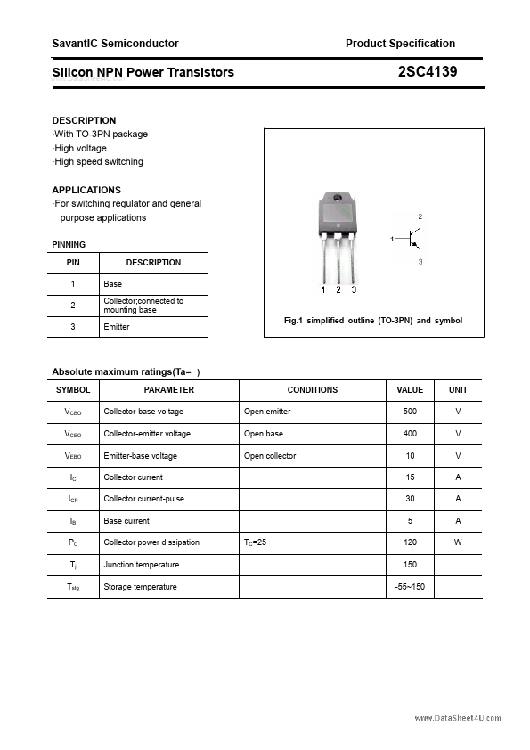
With TO-3PN package
High voltage
High speed switching APPLICATIONS
For switching regulator and general purpose applications
PINNING PIN 1 2 3 Base Collector;connected to mounting base Emitter Fig.1 simplified outline (TO-3PN) and symbol DESCRIPTION
Absolute maximum ratings(Ta= )
Full PDF Text Transcription for 2SC4139 (Reference)
Note: Below is a high-fidelity text extraction (approx. 800 characters) for
2SC4139. For precise diagrams, and layout, please refer to the original PDF.
SavantIC Semiconductor www.DataSheet4U.com 
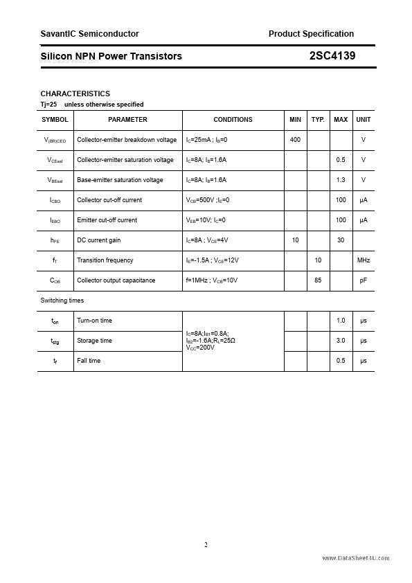
Product Specification Silicon NPN Power Transistors 2SC4139 DESCRIPTION ·With TO-3PN package ·High voltage ·High speed switchin...
View more extracted text
39 DESCRIPTION ·With TO-3PN package ·High voltage ·High speed switching APPLICATIONS ·For switching regulator and general purpose applications PINNING PIN 1 2 3 Base Collector;connected to mounting base Emitter Fig.1 simplified outline (TO-3PN) and symbol DESCRIPTION Absolute maximum ratings(Ta= ) SYMBOL VCBO VCEO VEBO IC ICP IB PC Tj Tstg PARAMETER Collector-base voltage Collector-emitter voltage Emitter-base voltage Collector current Collector current-pulse Base current Collector power dissipation Junction temperature Storage temperature TC=25 CONDITIONS Open emitter Open base Open collector VALUE 500 400 10 15 30 5 120