LH531000B-S
Overview
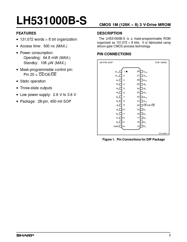
The LH531000B-S is a mask-programmable ROM organized as 131,072 × 8 bits. It is fabricated using silicon-gate CMOS process technology.
- 131,072 words × 8 bit organization
- Access time: 500 ns (MAX.)
- Power consumption: Operating: 64.8 mW (MAX.) Standby: 108 µW (MAX.)
- Mask-programmable control pin: Pin 20 = CE/OE/OE
- Static operation
- Three-state outputs
- Low power supply: 2.6 V to 3.6 V
- Package: 28-pin, 450-mil SOP