The following content is an automatically extracted verbatim text
from the original manufacturer datasheet and is provided for reference purposes only.
View original datasheet text
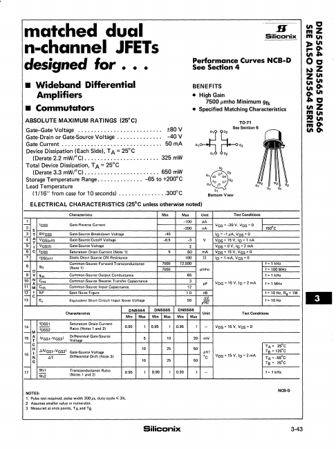
matched dual n-channel JFETs
H
Siliconix
designed for • • •
Performance Curves NCB-D See Sedion 4
• Wideband Differential Amplifiers
• Commutators
ABSOLUTE MAXIMUM RATINGS (25°C)
Gate-Gate Voltage .......................... ±80V
Gate-Drain or Gate-Source Voltage .....•..•••... -40 V Gate Current .....•.•••.•.••.•.•..•.•.....•.. 50 rnA Device Dissipation (Each Side), TA = 25°C
(Derate 2.2 mW/oC) ..•...••..•....•.•.••.• 325mW
Total Device Dissipation, TA = 25°C (Derate 3.3 mW/oC) •.••..•••••••.•.•.•..•. 650mW
Storage Temperature Range •••.•..••....• -65 to +200°C
Lead Temperature (1/16" from case for 10 seconds) ........•......