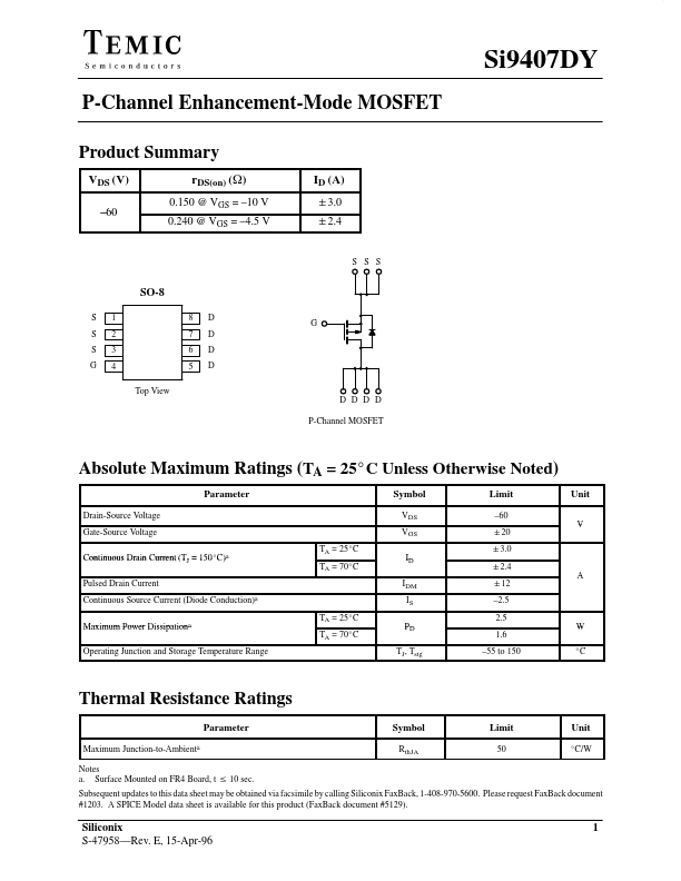
Si9407DY Description
Surface Mounted on FR4 Board, t v 10 sec. Subsequent updates to this data sheet may be obtained via facsimile by calling Siliconix FaxBack, 1-408-970-5600. Please request FaxBack document #1203.
Si9407DY is P-Channel MOSFET manufactured by TEMIC Semiconductors.
| Manufacturer | Part Number | Description |
|---|---|---|
| SI9407AEY | P-Channel MOSFET | |
| SI9407BDY-T1-GE3 | P-Channel MOSFET |
Surface Mounted on FR4 Board, t v 10 sec. Subsequent updates to this data sheet may be obtained via facsimile by calling Siliconix FaxBack, 1-408-970-5600. Please request FaxBack document #1203.