Download the 74HC74AF datasheet PDF.
This datasheet also covers the 74HC74AP variant, as both devices belong to the same dual d-type flip-flop family and are provided as variant models within a single manufacturer datasheet.
Key Features
High speed: fmax = 77 MHz (typ. ) at VCC = 5 V.
Low power dissipation: ICC = 2 μA (max) at Ta = 25°C.
High noise immunity: VNIH = VNIL = 28% VCC (min).
Output drive capability: 10 LSTTL loads.
Symmetrical output impedance: |IOH| = IOL = 4 mA (min).
Balanced propagation delays: tpLH ∼.
tpHL.
Wide operating voltage range: VCC (opr) = 2~6 V.
Pin and function compatible with 74LS74
Pin Assignment
Note: xxxFN (JEDEC SOP).
Note: The manufacturer provides a single datasheet file (74HC74AP_ToshibaSemiconductor.pdf) that lists specifications for multiple related part numbers.
Full PDF Text Transcription for 74HC74AF (Reference)
Note: Below is a high-fidelity text extraction (approx. 800 characters) for
74HC74AF. For precise diagrams, and layout, please refer to the original PDF.
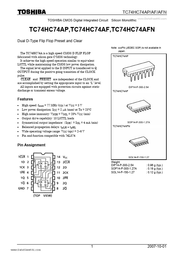
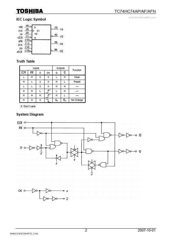
TC74HC74AP/AF/AFN TOSHIBA CMOS Digital Integrated Circuit Silicon Monolithic www.DataSheet4U.com TC74HC74AP,TC74HC74AF,TC74HC74AFN Dual D-Type Flip Flop Preset and Clear ...
View more extracted text
4HC74AP,TC74HC74AF,TC74HC74AFN Dual D-Type Flip Flop Preset and Clear The TC74HC74A is a high speed CMOS D FLIP FLOP fabricated with silicon gate C2MOS technology. It achieves the high speed operation similar to equivalent LSTTL while maintaining the CMOS low power dissipation. The signal level applied to the D INPUT is transferred to Q OUTPUT during the positive going transition of the CLOCK pulse. CLEAR and PRESET are independent of the CLOCK and are accomplished by setting the appropriate input to an “L” level. All inputs are equipped with protection circuits against static discharge or transient excess voltage. Feature