TB6561NG
Features
- Power supply voltage: 40 V (max)
- Output current: 1.5 A (max)
- Low ON-resistance: 1.5 Ω (upper and lower transistors/typ.)
- Direct PWM current control system
- Power-saving function
- Forward/reverse/short brake/stop modes
- Over-current protection: ILIM = 2.5 A (typ.)
- Thermal shutdown
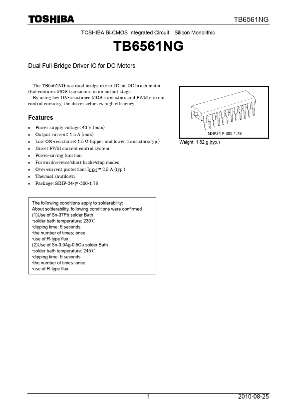
- Package: SDIP-24-P-300-1.78
Weight: 1.62 g (typ.)
The following conditions apply to solderability: About solderability, following conditions were confirmed (1)Use of Sn-37Pb solder Bath
- solder bath temperature: 230℃
- dipping time: 5 seconds
- the number of times: once
- use of R-type flux (2)Use of Sn-3.0Ag-0.5Cu solder Bath
- solder bath temperature: 245℃
- dipping time: 5 seconds
- the number of times: once
- use of R-type flux
2010-08-25
Block Diagram
Some of the functional blocks, circuits and constants in the block diagram may be omitted or simplified for explanatory purposes.
S-GND Vreg
VCC OUT2A
OUT1A OUT2B
VCC OUT1B S-GND
8...