Datasheet4U Logo Datasheet4U.com

TC518128BFL-10V - SILICON GATE CMOS PSEUDO STATIC RAM

Download the TC518128BFL-10V datasheet PDF. This datasheet also covers the TC518128BPL-70V variant, as both devices belong to the same silicon gate cmos pseudo static ram family and are provided as variant models within a single manufacturer datasheet.

General Description

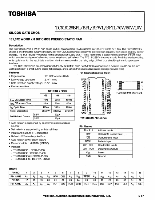
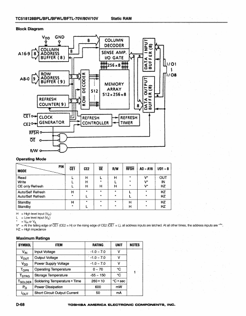
The TC518128B-V is a 1M bit high speed CMOS pseudo static RAM organized as 131,072 words by 8 bits.

utilizes a one transistor dynamic memory cell with CMOS peripheral circuitry to provide high capacity, high speed and low power storage.

Key Features

  • a static RAM-like interface with a write cycle in which the input data is written into the memory cell at the rising edge of RMI thus simplifying the microprocessor interface. The TC518128B-V is pin-compatible with the 1M bit CMOS static RAM JEDEC standard and is available in a 32-pin, 0.6 inch width plastic DIP, a small outline plastic flat package, and a 32-pin thin small outline plastic package (forward t.

📥 Download Datasheet

Note: The manufacturer provides a single datasheet file (TC518128BPL-70V-Toshiba.pdf) that lists specifications for multiple related part numbers.

Full PDF Text Transcription (Reference)

The following content is an automatically extracted verbatim text from the original manufacturer datasheet and is provided for reference purposes only.

View original datasheet text
TOSHIBA SILICON GATE CMOS TC518l28BPL/BFL/BFWL/BFIL-70V/80V/lOV 131,072 WORD x 8 BIT CMOS PSEUDO STATIC RAM Description The TC518128B-V is a 1M bit high speed CMOS pseudo static RAM organized as 131,072 words by 8 bits. The TC518128B-V utilizes a one transistor dynamic memory cell with CMOS peripheral circuitry to provide high capacity, high speed and low power storage. The TC518128B-Voperates from a single power supply of 2.7 - 5.5V. Refreshing is supported by a refresh (RFS~ input which enables two types of refreshing - auto refresh and self refresh. The TC518128B-V features a static RAM-like interface with a write cycle in which the input data is written into the memory cell at the rising edge of RMI thus simplifying the microprocessor interface.