TC74VHC9126P
TC74VHC9126P is 5-bit Universal Schmitt Buffer manufactured by Toshiba.
- Part of the TC74VHC9125P comparator family.
- Part of the TC74VHC9125P comparator family.
TC74VHC9125,9126P/FK
TOSHIBA CMOS Digital Integrated Circuit Silicon Monolithic
TC74VHC9125P, TC74VHC9125FK TC74VHC9126P, TC74VHC9126FK
TC74VHC9125P/FK 5-bit Universal Schmitt Buffer with 3-State Outputs TC74VHC9126P/FK 5-bit Universal Schmitt Buffer with 3-State Outputs
The TC74VHC9125/9126 are an ultra-high-speed 5-bit Schmitt buffer fabricated using silicon-gate CMOS technology. The TC74VHC9125/9126 bines low power consumption of CMOS with Schottky TTL speeds.
Y1 to Y4 outputs can be put in the high-impedance state by placing a logic HIGH on the Enable ( G ) input. The CONT input determines the logical inversion of data. A logic LOW on the CONT input configures the TC74VHC9125/9126 as an inverter; a logic HIGH on the CONT input configures the TC74VHC9125/9126 as a buffer.
TC74VHC9125 Y5 output is an inverting type, and the TC74VHC9126 Y5 output is a non-inverting type.
All the inputs have hysteresis between the positive-going and negativegoing thresholds. Thus the TC74VHC9125/9126 are capable of squaring up transitions of slowly changing input signals and provides an improved noise immunity.
Additionally, all the inputs have a newly developed protection circuit without a diode returned to VCC. This enables the inputs to be tolerant of up to 5 volts even when power supply is down. The input power-down protection capability makes the TC74VHC9125/9126 ideal for a wide range of applications, such as interfacing between different voltages, voltage translation from 5 V to 3 V and battery back-up circuits.
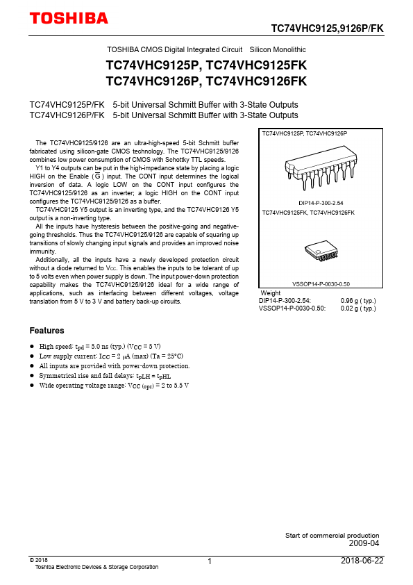
TC74VHC9125P, TC74VHC9126P
TC74VHC9125FK, TC74VHC9126FK
Weight DIP14-P-300-2.54: VSSOP14-P-0030-0.50:
0.96 g ( typ.) 0.02 g ( typ.)
Features
- High speed: tpd = 5.0 ns (typ.) (VCC = 5 V)
- Low supply current: ICC = 2 µA (max) (Ta = 25°C)
- All inputs are provided with power-down protection.
- Symmetrical rise and fall delays: tp LH ∼- tp HL
- Wide operating voltage range: VCC (opr) = 2 to 5.5 V
© 2018
Toshiba Electronic Devices & Storage Corporation
Sta...