Datasheet4U.com
🌙
TC7SG07FE Datasheet | Toshiba
Part:
TC7SG07FE
Description:
Non-Inverter
Manufacturer:
Toshiba
Size:
196.33 KB
TC7SG07FE Datasheet (PDF) Download
Related TC7SG07FE Datasheets
TC7SG07AFS Non-Inverter
TC7SG02FU 2-Input NOR Gate
TC7SG00AFS 2-Input NAND Gate
TC7SG08AFS 2-Input AND Gate
TC7SG05AFS Inverter
Toshiba
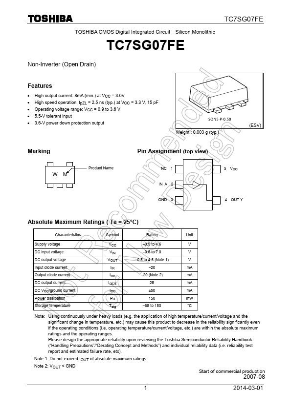
TC7SG07FE
Key Features
High output current: 8mA (min.) at VCC = 3.0V
High speed operation: tpZL = 2.5 ns (typ.) at VCC = 3.3 V, 15 pF
Operating voltage range: VCC = 0.9 to 3.6 V
5.5-V tolerant input
3.6-V power down protection output
×
Close