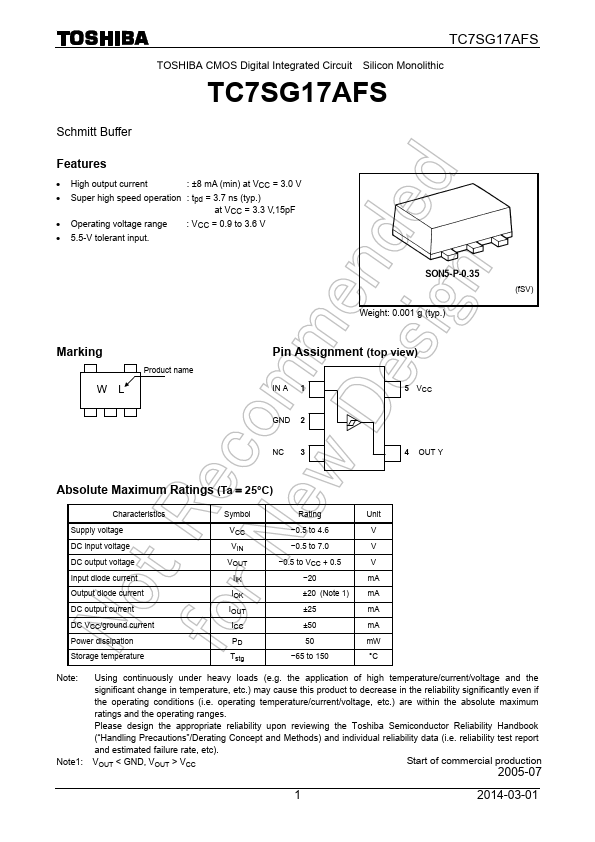
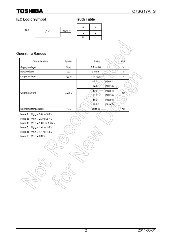
TC7SG17AFS
TOSHIBA CMOS Digital Integrated Circuit Silicon Monolithic
TC7SG17AFS
Schmitt Buffer
Features
• High output current
: ±8 mA (min) at VCC = 3.0 V
• Super high speed operation : tpd = 3.7 ns (typ.)
at VCC = 3.3 V,15pF
• Operating voltage range : VCC = 0.9 to 3.6 V
• 5.5-V tolerant input.
SON5-P-0.35
Weight: 0.001 g (typ.)
(fSV)
Marking
WL
Product name
Pin Assignment (top view)
IN A 1
GND 2
NC 3
5 VCC
4 OUT Y
Absolute Maximum Ratings (Ta = 25°C)
Characteristics
Supply voltage
DC input voltage
DC output voltage
Input diode current
Output diode current
DC output current
DC VCC/ground current
Power dissipation
Storage temperature
Symbol
VCC
VIN
VOUT
IIK
IOK
IOUT
ICC
PD
Tstg
Rating
Unit
−0.5 to 4.6
V
−0.5 to 7.0
V
−0.5 to VCC + 0.5
V
−20
mA
±20 (Note 1) mA
±25
mA
±50
mA
50
mW
−65 to 150
°C
Note:
Note1:
Using continuously under heavy loads (e.g. the application of high temperature/current/voltage and the
significant change in temperature, etc.) may cause this product to decrease in the reliability significantly even if
the operating conditions (i.e. operating temperature/current/voltage, etc.) are within the absolute maximum
ratings and the operating ranges.
Please design the appropriate reliability upon reviewing the Toshiba Semiconductor Reliability Handbook
(“Handling Precautions”/Derating Concept and Methods) and individual reliability data (i.e. reliability test report
and estimated failure rate, etc).
VOUT < GND, VOUT > VCC
Start of commercial production
2005-07
1
2014-03-01