Datasheet4U.com
🌙
TC7SPB9306TU
TC7SPB9307TU
TC7SPB9306TU Datasheet | Toshiba
Part:
TC7SPB9306TU
Description:
1-Bit Dual-Supply Bus Switch
Manufacturer:
Toshiba
Size:
309.96 KB
TC7SPB9306TU Datasheet (PDF) Download
Toshiba
TC7SPB9306TU
Key Features
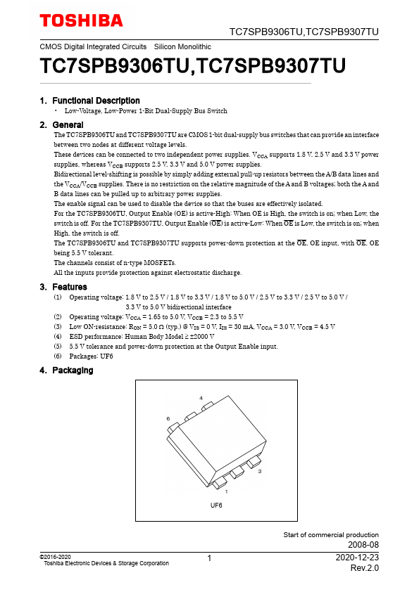
Pin Assignment TC7SPB9306TU TC7SPB9306TU,TC7SPB9307TU TC7SPB9307TU
Marking TC7SPB9306TU TC7SPB9307TU
×
Close