Datasheet4U.com
🌙
TC7WZ126FU Datasheet | Toshiba
Part:
TC7WZ126FU
Description:
Dual Bus Buffer
Manufacturer:
Toshiba
Size:
157.39 KB
TC7WZ126FU Datasheet (PDF) Download
Related TC7WZ126FU Datasheets
TC7WZ126FK Dual Bus Buffer
TC7WZ125FK Dual Bus Buffer
TC7WZ125FU Dual Bus Buffer
Toshiba
TC7WZ126FU
Key Features
(1) Wide operating temperature range: Topr = -40 to 125 (Note
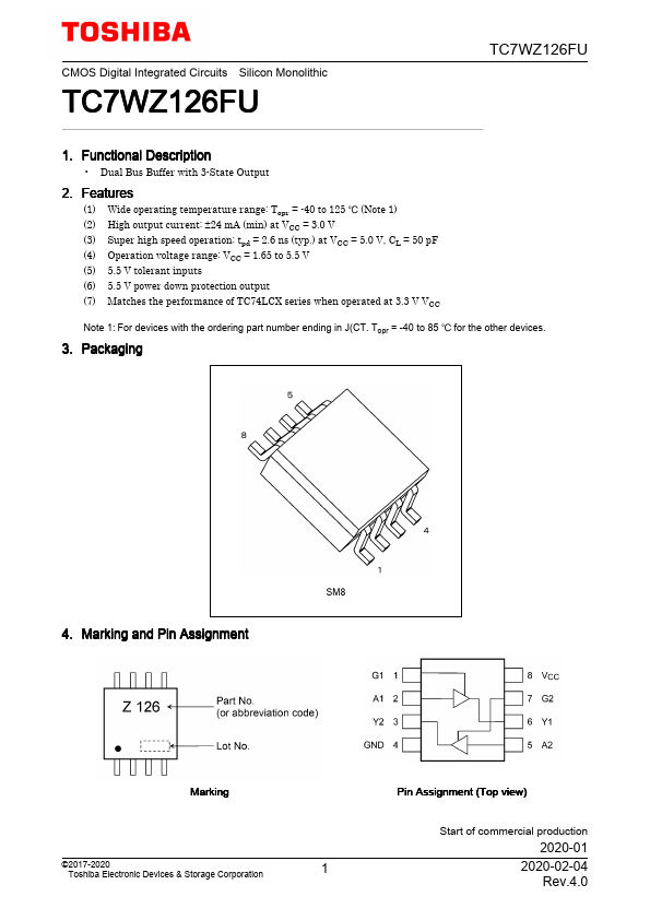
Packaging SM8
IEC Logic Symbol TC7WZ126FU
Truth Table Input A X L H Input G L H H Output Y
L H X: Don't care Z: High impedance
×
Close