2SK3376MFV
2SK3376MFV is N-Channel MOSFET manufactured by Toshiba.
TOSHIBA Field Effect Transistor Silicon N Channel Junction Type
For ECM
- Application for Ultra-pact ECM
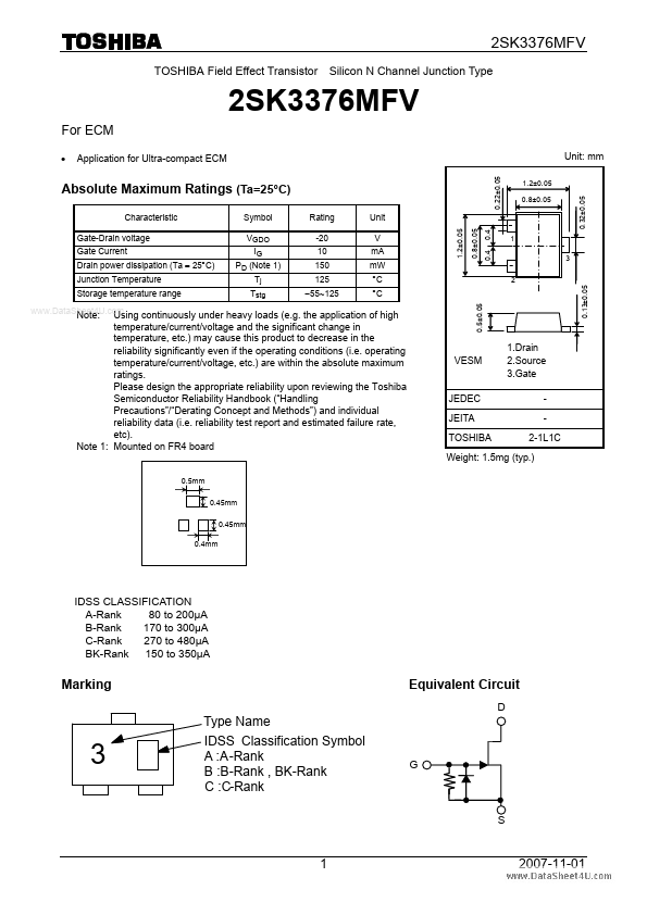
0.22±0.05 1.2±0.05 0.32±0.05 3 2 0.13±0.05 0.8±0.05
Unit: mm
Absolute Maximum Ratings (Ta=25°C)
Characteristic Gate-Drain voltage Gate Current Drain power dissipation (Ta = 25°C) Junction Temperature Storage temperature range Symbol VGDO IG PD (Note 1) Tj Tstg Rating -20 10 150 125
- 55~125 Unit
1.2±0.05 0.8±0.05
V m A m W °C °C
.. Note: Using continuously under heavy loads (e.g. the application of high temperature/current/voltage and the significant change in temperature, etc.) may cause this product to decrease in the reliability significantly even if the operating conditions (i.e. operating temperature/current/voltage, etc.) are within the absolute maximum ratings. Please design the appropriate reliability upon reviewing the Toshiba Semiconductor Reliability Handbook (“Handling Precautions”/“Derating Concept and Methods”) and individual reliability data (i.e. reliability test report and estimated failure rate, etc). Note 1: Mounted on FR4 board
0.5±0.05
VESM
1.Drain 2.Source 3.Gate 2-1L1C
JEDEC JEITA TOSHIBA
Weight: 1.5mg (typ.)
0.5mm 0.45mm 0.45mm 0.4mm
IDSS CLASSIFICATION A-Rank 80 to 200µA B-Rank 170 to 300µA C-Rank 270 to 480µA BK-Rank 150 to 350µA
Marking Type Name
Equivalent Circuit
IDSS Classification Symbol A :A -Rank B :B-Rank , BK-Rank C :C-Rank
2007-11-01
Electrical Characteristics (A-Rank IDSS Ta=25°C)
Characteristic Drain Current Drain Current Gate-Source Cut-off Voltage Forward transfer admittance Input capacitance Voltage Gain Delta Voltage Gain Delta Voltage Gain Noise Voltage Symbol IDSS ID Test Condition VDS = 2 V, VGS = 0 VDD = 2 V, RL= 2kΩ,Cg = 3p F Min 80 ⎯ -0.1 0.7 ⎯ -13.5 ⎯ ⎯ ⎯ Typ. ⎯ ⎯ ⎯ 1.4 5.5 ⎯ ⎯ ⎯ ⎯ Max 200 240 -0.8 ⎯ ⎯ -9.0 -2.0 -4.0 47 Unit µA µA V m S p F d B d B d B m V
VGS(OFF) VDS = 2 V, ID = 1μA |Yfs| Ciss Gv DGv(f) VDS = 2 V,VGS = 0V VDS = 2 V, VGS = 0, f =...