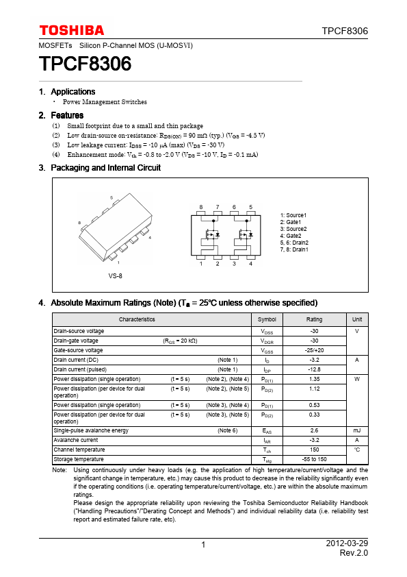
Datasheet4U Logo Datasheet4U.com

TPCF8306 - MOSFET

Key Features

  • (1) (2) (3) (4) Small footprint due to a small and thin package Low drain-source on-resistance: RDS(ON) = 90 mΩ (typ. ) (VGS = -4.5 V) Low leakage current: IDSS = -10 µA (max) (VDS = -30 V) Enhancement mode: Vth = -0.8 to -2.0 V (VDS = -10 V, ID = -0.1 mA) 3. Packaging and Internal Circuit 1: Source1 2: Gate1 3: Source2 4: Gate2 5, 6: Drain2 7, 8: Drain1 VS-8 4. Absolute Maximum Ratings (Note) (Ta = 25 unless otherwise specified) Characteristics Drain-source voltage Drain-gate voltage Gate-s.

📥 Download Datasheet

Full PDF Text Transcription (Reference)

The following content is an automatically extracted verbatim text from the original manufacturer datasheet and is provided for reference purposes only.

View original datasheet text
TPCF8306 MOSFETs Silicon P-Channel MOS (U-MOS) TPCF8306 1. Applications • Power Management Switches 2. Features (1) (2) (3) (4) Small footprint due to a small and thin package Low drain-source on-resistance: RDS(ON) = 90 mΩ (typ.) (VGS = -4.5 V) Low leakage current: IDSS = -10 µA (max) (VDS = -30 V) Enhancement mode: Vth = -0.8 to -2.0 V (VDS = -10 V, ID = -0.1 mA) 3. Packaging and Internal Circuit 1: Source1 2: Gate1 3: Source2 4: Gate2 5, 6: Drain2 7, 8: Drain1 VS-8 4.