MA4BPS201
MA4BPS201 is PIN Diode Chips with Offset Bond Pads manufactured by Tyco Electronics.
PIN Diode Chips With Offset Bond Pads
MA4BPS101, MA4BPS201, MA4BPS301
MA4BPS101, MA4BPS201, MA4BPS301
PIN Diode Chips with Offset Bond Pads
Features
- -
- -
- Bond Pads Removed From Active Junction Large Bond Pads Support Multiple Bond Wires Rugged Silicon-Glass Construction Silicon Nitride Passivation Polyimide Scratch Protection
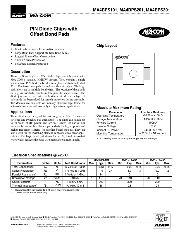
Chip Layout
Description
These silicon
- glass PIN diode chips are fabricated with M/A-’s patented HMIC™ process. They contain a single shunt silicon PIN diode embedded in a glass substrate with dual 75 x 150 micron bond pads located near the chip edges. The large pads allow use of multiple bond wires. The location of these pads on a glass substrate...