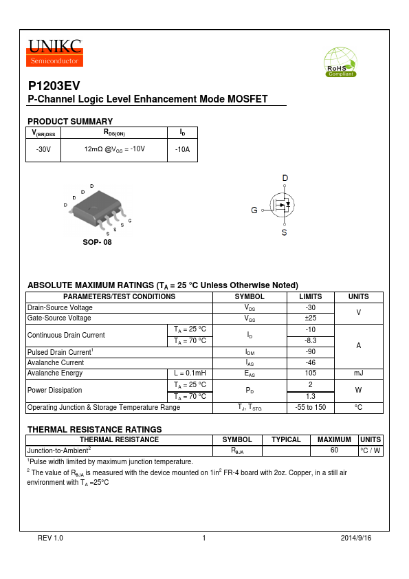
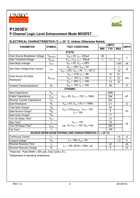
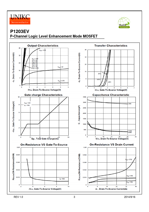
Click to expand full text
P1203EV
P-Channel Logic Level Enhancement Mode MOSFET
PRODUCT SUMMARY
V(BR)DSS
RDS(ON)
-30V
12mΩ @VGS = -10V
ID -10A
SOP- 08
ABSOLUTE MAXIMUM RATINGS (TA = 25 °C Unless Otherwise Noted)
PARAMETERS/TEST CONDITIONS
SYMBOL
LIMITS
Drain-Source Voltage
VDS -30
Gate-Source Voltage
VGS ±25
Continuous Drain Current Pulsed Drain Current1
TA = 25 °C TA = 70 °C
ID IDM
-10 -8.3 -90
Avalanche Current
IAS -46
Avalanche Energy
L = 0.1mH
EAS
105
Power Dissipation
TA = 25 °C TA = 70 °C
PD
2 1.3
Operating Junction & Storage Temperature Range
TJ, TSTG
-55 to 150
UNITS V
A
mJ W °C
THERMAL RESISTANCE RATINGS
THERMAL RESISTANCE
SYMBOL
TYPICAL MAXIMUM
Junction-to-Ambient2
RqJA
60
1Pulse width limited by maximum junction temperature.