Datasheet Summary
UNISONIC TECHNOLOGIES CO., LTD
PNP EPITAXIAL SILICON TRANSISTOR
NPN SILICON EPITAXIAL TRANSISTOR
- DESCRIPTION
The UTC 2SC5006 is an NPN epitaxial transistor; it uses UTC’s advanced technology to provide the customers with low noise figure, high DC current gain and high current capability achieve a very wide dynamic range and excellent linearity.
The UTC 2SC5006 is suitable for low noise and small signal amplifiers from VHF band to UHF band.
- Features
- High DC current gain
- High current capability
- Low noise figure
2 1
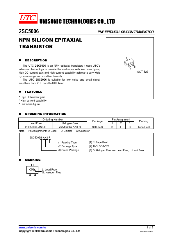
SOT-523
- ORDERING INFORMATION
Ordering Number
Lead Free
Halogen-Free
2SC5006L-AN3-R
2SC5006G-AN3-R
Note: Pin Assignment: B: Base E: Emitter C:...