1N5550
Overview
- Cavity-free glass passivated junction
- High temperature metallurgically bonded con- struction
- Hermetically sealed package
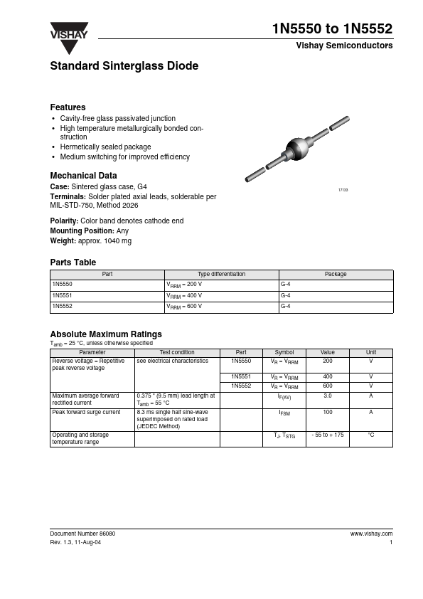
- Medium switching for improved efficiency Mechanical Data Case: Sintered glass case, G4 Terminals: Solder plated axial leads, solderable per MIL-STD-750, Method 2026 Polarity: Color band denotes cathode end Mounting Position: Any Weight: approx. 1040 mg 17133 Parts Table Part 1N5550 1N5551 1N5552 Type differentiation Package VRRM = 200 V G-4 VRRM = 400 V G-4 VRRM = 600 V G-4