WCMC1616V9X
Overview
- 1T Cell, PSRAM Architecture
- High speed: 70 ns
- Wide Voltage range: - VCC range: 2.7V to 3.3V
- Low active power - Typical active current: 2 mA @ f = 1 MHz - Typical active current: 13 mA @ f = fMAX
- Low standby power
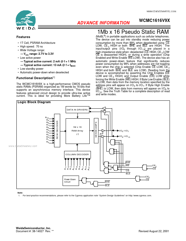
- Automatic power-down when deselected Functional Description[1] The WCMC1616V9X is a high-performance CMOS pseudo static RAMs (PSRAM) organized as 1M words by 16 bits that supports an asynchronous memory interface. This device features advanced circuit design to provide ultra-low active current. This is ideal for providing More Battery Life TM (MoBL® ) in portable applications such as cellular telephones. The device can be put into standby mode reducing power consumption by more than 99% when deselected using CE LOW, CE 2 HIGH or both BHE and BLE are HIGH. The input/output pins (I/O0 through I/O 1 5) are placed in a high-impedance state when: deselected (CE HIGH, CE 2 LOW OE is deasserted HIGH), or during a write operation (Chip Enabled and Write Enable WE LOW). The device also has an automatic power-down feature that significantly reduces power consumption by 99% when addresses are not toggling even when the chip is selected (Chip Enable CE LOW, CE 2 HIGH and both BHE and BLE are LOW). Reading from the device is accomplished by asserting the Chip Enables (CE LOW and CE 2 HIGH) and Output Enable (OE) LOW while forcing the Write Enable (WE) HIGH. If Byte Low Enable (BLE) is LOW, then data from the memory location specified by the address pins will appear on I/O 0 to I/O
- If Byte High Enable (BHE ) is LOW, then data from memory will appear on I/O8 to I/O 15 . See the Truth Table for a complete description of read and write modes. 1Mb x 16 Pseudo Static RAM Logic Block Diagram