ADS4122, ADS4125, ADS4142, ADS4145
SBAS520C – FEBRUARY 2011 – REVISED JUNE 2017
www.ti.com
Table of Contents
1 Features .................................................................. 1
2 Applications ........................................................... 1
3 Description ............................................................. 1
4 Revision History..................................................... 2
5 Device Family Comparison................................... 4
6 Pin Configuration and Functions ......................... 4
7 Specifications......................................................... 7
7.1 Absolute Maximum Ratings ...................................... 7
7.2 ESD Ratings.............................................................. 7
7.3 Recommended Operating Conditions....................... 8
7.4 Thermal Information .................................................. 8
7.5 Electrical Characteristics: ADS412x ......................... 9
7.6 Electrical Characteristics: ADS414x ....................... 11
7.7 Electrical Characteristics: General .......................... 13
7.8 Digital Characteristics ............................................. 14
7.9 Timing Requirements: LVDS and CMOS Modes.... 14
7.10 Serial Interface Timing Characteristics ................. 15
7.11 Reset Timing Requirements ................................. 16
7.12 Timing Characteristics at Lower Sampling
Frequencies ............................................................. 16
7.13 Typical Characteristics: ADS4122 ........................ 19
7.14 Typical Characteristics: ADS4125 ........................ 22
7.15 Typical Characteristics: ADS4142 ........................ 25
7.16 Typical Characteristics: ADS4145 ........................ 29
7.17 Typical Characteristics: Common ......................... 33
7.18 Typical Characteristics: Contour ........................... 34
8 Detailed Description ............................................ 35
8.1 Overview ................................................................. 35
8.2 Functional Block Diagrams .................................... 36
8.3 Feature Description................................................. 38
8.4 Device Functional Modes........................................ 40
8.5 Programming........................................................... 46
8.6 Register Maps ......................................................... 49
9 Application and Implementation ........................ 57
9.1 Application Information............................................ 57
9.2 Typical Application .................................................. 72
10 Power Supply Recommendations ..................... 74
10.1 Sharing DRVDD and AVDD Supplies ................... 74
10.2 Using DC-DC Power Supplies .............................. 74
10.3 Power Supply Bypassing ...................................... 74
11 Layout................................................................... 74
11.1 Layout Guidelines ................................................. 74
11.2 Layout Example .................................................... 75
12 Device and Documentation Support ................. 76
12.1 Device Support...................................................... 76
12.2 Documentation Support ........................................ 78
12.3 Related Links ........................................................ 78
12.4 Receiving Notification of Documentation Updates 78
12.5 Community Resources.......................................... 78
12.6 Trademarks ........................................................... 78
12.7 Electrostatic Discharge Caution ............................ 78
12.8 Glossary ................................................................ 79
13 Mechanical, Packaging, and Orderable
Information ........................................................... 79
4 Revision History
NOTE: Page numbers for previous revisions may differ from page numbers in the current version.
Changes from Revision B (January 2016) to Revision C
Page
• Added a new feature Idle Channel SNR 74.8 dBFS (ADS414x)
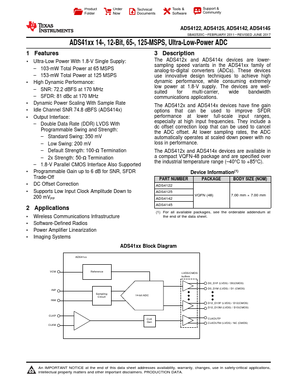
 to the Features section...................................................... 1
• Added a new application Imaging Systems in Applications section....................................................................................... 1
• Changed ADS412x/4x to ADS412x and ADS414x in Description section ............................................................................. 1
• Changed ADS41xx Block Diagram in the first page............................................................................................................... 1
• Changed input clock sample rate minimum for the ADS4122/ADS4142, low-speed mode enabled by default from:
20 MSPS to: 3 MSPS ............................................................................................................................................................ 8
• Changed input clock sample rate minimum for the ADS4122/ADS4142, low-speed mode enabled from: 20 MSPS to:
3 MSPS ................................................................................................................................................................................. 8
• Deleted High Performance Modes section from Recommended Operating Conditions table, moved to Programming
section .................................................................................................................................................................................... 8
• Added order to HD2 and HD3 parameter names in Electrical Characteristics tables.......................................................... 10
• Added test conditions header to Electrical Characteristics: General table .......................................................................... 13
• Added Using the ADS41xx at Low Sampling Rates subsection in Application and Implementation section....................... 62
• Added Figure 114 to Figure 124 in ADS412x (12-Bit Device) section ................................................................................. 62
• Changed the order of figures in ADS412x (12-Bit Device) section. .................................................................................... 62
• Added the device name ADS412x to the conditions of ADS412x (12-Bit Device) section. ................................................. 62
• Changed the unit of fS from MHz to MSPS in the specifications of Figure 115 ................................................................... 62
• Added new subsection ADS412x (12-Bit Device) in Application Information section. ........................................................ 62
2 Submit Documentation Feedback
Copyright © 2011–2017, Texas Instruments Incorporated
Product Folder Links: ADS4122 ADS4125 ADS4142 ADS4145