Datasheet Summary
CDCV850, CDCV850I 2.5ĆV PHASE LOCK LOOP CLOCK DRIVER
WITH 2ĆLINE SERIAL INTERFACE
SCAS647B
- OCTOBER 2000
- REVISED DECEMBER 2002
D Phase-Lock Loop Clock Driver for Double
Data-Rate Synchronous DRAM
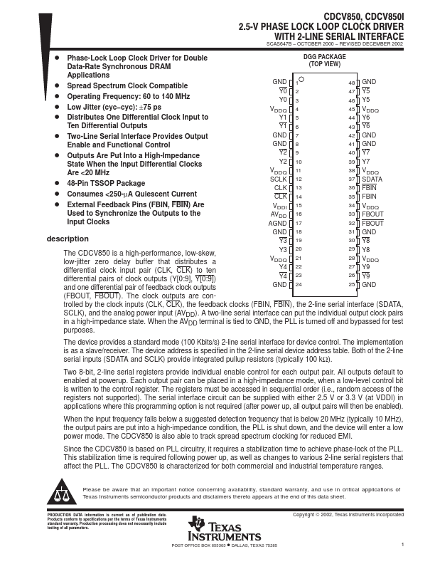
DGG PACKAGE (TOP VIEW)
Applications
D Spread Spectrum Clock patible D Operating Frequency: 60 to 140 MHz D Low Jitter (cyc- cyc): ±75 ps D Distributes One Differential Clock Input to
GND 1 Y0 2 Y0 3
VDDQ 4 Y1 5
48 GND 47 Y5 46 Y5 45 VDDQ 44 Y6
Ten Differential Outputs
Y1 6
43 Y6
D Two-Line Serial Interface Provides Output
Enable and Functional Control
D Outputs Are Put Into a High-Impedance
State When the Input Differential Clocks Are <20 MHz
D 48-Pin TSSOP Package D Consumes <250-µA...