CDCV857A Overview
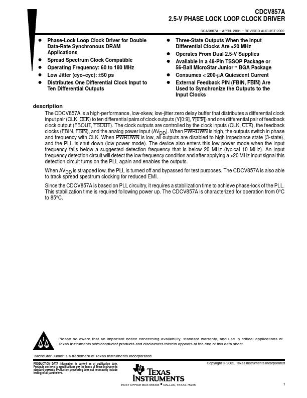
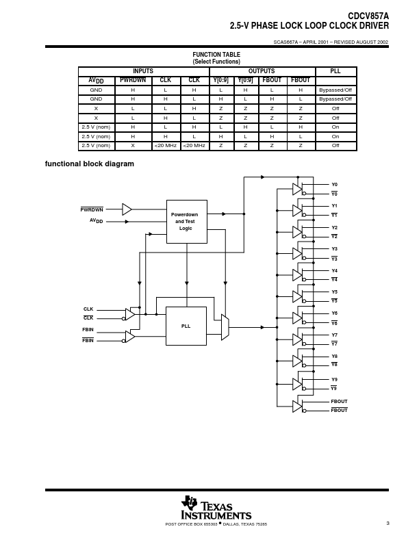
The CDCV857A is a high-performance, low-skew, low-jitter zero delay buffer that distributes a differential clock input pair (CLK, CLK) to ten differential pairs of clock outputs (Y[0:9], Y[0:9]) and one differential pair of feedback clock output (FBOUT, FBOUT). The clock outputs are controlled by the clock inputs (CLK, CLK), the feedback clocks (FBIN, FBIN), and the analog power input (AVDD). When PWRDWN is high,...


