Datasheet4U Logo Datasheet4U.com

CDCV857BI - 2.5-V PHASE LOCK LOOP CLOCK DRIVER

Download the CDCV857BI datasheet PDF. This datasheet also covers the CDCV857B variant, as both devices belong to the same 2.5-v phase lock loop clock driver family and are provided as variant models within a single manufacturer datasheet.

General Description

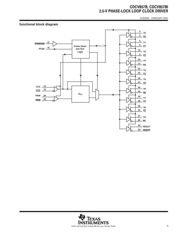
The CDCV857B is a high-performance, low-skew, low-jitter zero delay buffer that distributes a differential clock input pair (CLK, CLK) to 10 differential pairs of clock outputs (Y[0:9], Y[0:9]) and one differential pair of feedback clock outputs (FBOUT, FBOUT).

📥 Download Datasheet

Note: The manufacturer provides a single datasheet file (CDCV857B-etcTI.pdf) that lists specifications for multiple related part numbers.

Full PDF Text Transcription (Reference)

The following content is an automatically extracted verbatim text from the original manufacturer datasheet and is provided for reference purposes only.

View original datasheet text
CDCV857B, CDCV857BI 2.5ĆV PHASEĆLOCK LOOP CLOCK DRIVER D Phase-Lock Loop Clock Driver for Double Data-Rate Synchronous DRAM Applications D Spread Spectrum Clock Compatible D Operating Frequency: 60 MHz to 200 MHz D Low Jitter (cycle-cycle): ±50 ps D Low Static Phase Offset: ±50 ps D Low Jitter (Period): ±35 ps D Distributes One Differential Clock Input to 10 Differential Outputs SCAS689 − FEBRUARY 2003 D Enters Low-Power Mode When No CLK Input Signal Is Applied or PWRDWN Is Low D Operates From Dual 2.