CDCV850I Overview
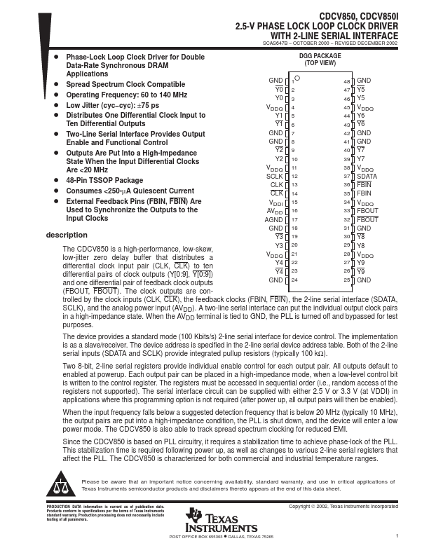
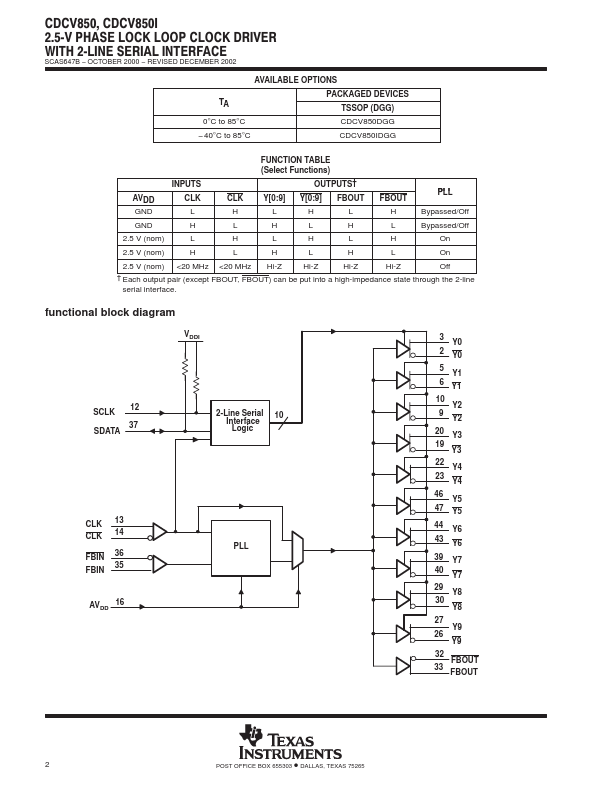
The clock outputs are con- trolled by the clock inputs (CLK, CLK), the feedback clocks (FBIN, FBIN), the 2-line serial interface (SDATA, SCLK), and the analog power input (AVDD). A two-line serial interface can put the individual output clock pairs in a high-impedance state. When the AVDD terminal is tied to GND, the PLL is turned off and bypassed for test purposes.