CSD13302W
Description
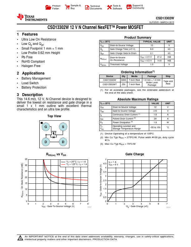
This 14.6 mΩ, 12 V, N-Channel device is designed to deliver the lowest on resistance and gate charge in a small 1 x 1 mm outline with excellent Top View Product Summary TA = 25°C VDS Drain-to-Source Voltage Qg Gate Charge Total (4.5 V) Qgd Gate Charge Gate-to-Drain RDS(on) Drain-to-Source On-Resistance VGS(th) Threshold Voltage TYPICAL VALUE 12 6.0 2.1 VGS = 2.5 V VGS = 4.5 V 1.0 21.2 14.6 UNIT V nC nC mΩ mΩ V Device CSD13302W CSD13302WT.
Key Features
- 1 Ultra Low On Resistance
- Low Qg and Qgd
- Small Footprint 1 mm × 1 mm
- Low Profile 0.62 mm Height
- RoHS compliant
- Halogen Free