CSD13306W
CSD13306W is 12-V N-Channel Power MOSFET manufactured by Texas Instruments.
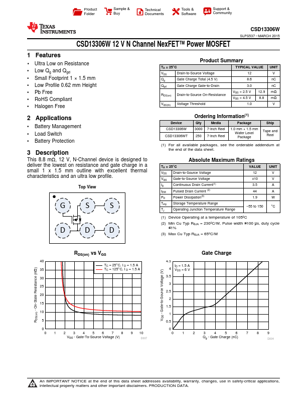
Product Folder
Sample & Buy
Technical Documents
Tools & Software
Support & munity
CSD13306W 12 V N Channel NexFET™ Power MOSFET
SLPS537
- MARCH 2015
1 Features
- 1 Ultra Low on Resistance
- Low Qg and Qgd
- Small Footprint 1 × 1.5 mm
- Low Profile 0.62 mm Height
- Pb Free
- RoHS pliant
- Halogen Free
2 Applications
- Battery Management
- Load Switch
- Battery Protection
3 Description
This 8.8 mΩ, 12 V, N-Channel device is designed to deliver the lowest on resistance and gate charge in a small 1 x 1.5 mm outline with excellent thermal characteristics and an ultra low profile.
Top View
Product Summary
TA = 25°C
Drain-to-Source Voltage
Qg
Gate Charge...