CSD22206WT Overview
Key Specifications
Pins: 9
Height: 625 µm
Length: 1.75 mm
Width: 1.75 mm
Description
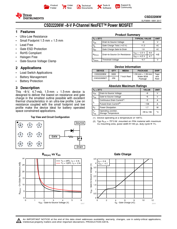
This –8-V, 4.7-mΩ, 1.5-mm × 1.5-mm device is designed to deliver the lowest on resistance and gate charge in the smallest outline possible with excellent Top View and Circuit Configuration G S S Source DEVICE CSD22206W CSD22206WT Device Information QTY MEDIA PACKAGE 3000 250 1.50-mm × 1.50-mm 7-Inch Reel Wafer BGA Package SHIP Tape and Reel TA = 25°C VDS Drain-to-Source Voltage VGS Gate-to-Source Voltage Continuous Drain Current(1) ID Pulsed Drain Current(2) VALUE –8 –6 –5 –108 UNIT V V A A PD Power Dissipation TJ, Operating Junction, Tstg Storage Temperature 1.7 W –55 to 150 °C (1) Device operating at a temperature of 105°C. (2) Typ RθJA = 75°C/W ,mounted on FR4 material with maximum Cu mounting area, pulse width ≤ 100 μs, duty cycle ≤ 1%.
Key Features
- 1 Ultra-Low Resistance
- Small Footprint 1.5 mm × 1.5 mm
- Gate ESD Protection
- RoHS Compliant
- Halogen Free