SN54HCT125
SN54HCT125 is QUADRUPLE BUS BUFFER GATE manufactured by Texas Instruments.
SN54HCT125, SN74HCT125
SCLS069G
- NOVEMBER 1988
- REVISED OCTOBER 2022
SNx4HCT125 Quadruple Bus Buffer Gates With 3-State Outputs
1 Features
- Operating voltage range of 4.5 V to 5.5 V
- High-current can drive up to 15 LSTTL loads
- Low power consumption, 80-µA max ICC
- Typical tpd = 12 ns
- ±6-mA output drive at 5 V
- Low input current of 1 µA max
- Inputs are TTL-voltage patible
- High-current 3-state outputs drive bus lines or buffer memory address registers
2 Description
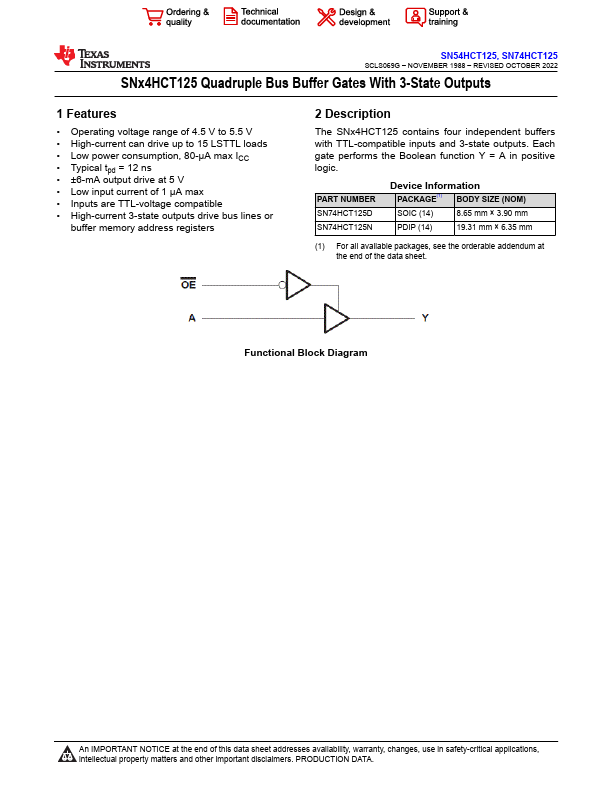
The SNx4HCT125 contains four independent buffers with TTL-patible inputs and 3-state outputs. Each gate performs the Boolean function Y = A in positive logic.
PART NUMBER SN74HCT125D SN74HCT125N
Device...