SN65LVDS180
SN65LVDS180 is HIGH-SPEED DIFFERENTIAL LINE DRIVERS/RECEIVERS manufactured by Texas Instruments.
- Part of the SN65LVDS179 comparator family.
- Part of the SN65LVDS179 comparator family.
Features
- 1 Meets or Exceeds the Requirements of ANSI TIA/EIA-644-1995 Standard
- Full-Duplex Signaling Rates up to 150 Mbps (See Table 1)
- Bus-Pin ESD Exceeds 12 k V
- Operates From a Single 3.3-V Supply
- Low-Voltage Differential Signaling With Typical
Output Voltages of 350 m V and a 100-Ω Load
- Propagation Delay Times
- Driver: 1.7 ns Typical
- Receiver: 3.7 ns Typical
- Power Dissipation at 200 MHz
- Driver: 25 m W Typical
- Receiver: 60 m W Typical
- LVTTL Input Levels Are 5-V Tolerant
- Receiver Maintains High Input Impedance With VCC < 1.5 V
- Receiver Has Open-Circuit Fail Safe
2 Applications
- Wireless Infrastructure
- Tele Infrastructure
- Printer
3 Description
The SN65LVDS179, SN65LVDS180, SN65LVDS050, and SN65LVDS051 devices are differential line drivers and receivers that use low-voltage differential signaling (LVDS) to achieve signaling rates as high as 400 Mbps (see Table 1). The TIA/EIA-644 standard-pliant electrical interface provides a minimum differential output voltage magnitude of 247 m V into a 100-Ω load and receipt of 100-m V signals with up to 1 V of ground potential difference between a transmitter and receiver.
Device Information(1)
PART NUMBER PACKAGE
BODY SIZE (NOM)
SN65LVDS179
SOIC (8) VSSOP (8)
4.90 mm × 3.91 mm 3.00 mm × 3.00 mm
SOIC (14) TSSOP (14)
8.65 mm × 3.91 mm 5.00 mm × 4.40 mm
SN65LVDS050
SOIC (16) TSSOP (16)
9.90 mm × 3.91 mm 5.00 mm × 4.40 mm
SN65LVDS051
SOIC (16) TSSOP (16)
9.90 mm × 3.91 mm 5.00 mm × 4.40 mm
(1) For all available packages, see the orderable addendum at the end of the data sheet.
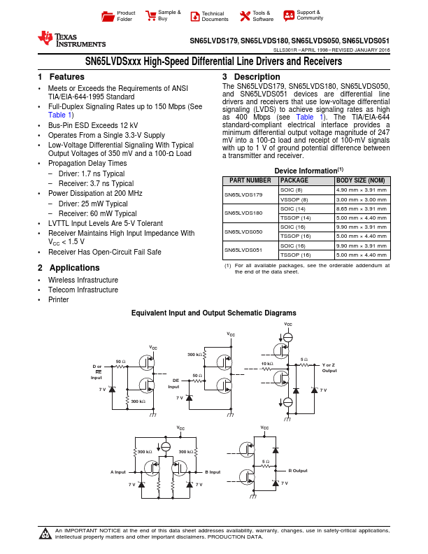
Equivalent Input and Output Schematic Diagrams
VCC VCC
D or...