• Part: SN65LVP19
  • Description: 2.5-V/3.3-V OSCILLATOR GAIN STAGE/BUFFERS
  • Manufacturer: Texas Instruments
  • Size: 879.07 KB
Download SN65LVP19 Datasheet PDF
Texas Instruments
SN65LVP19
FEATURES - Low-Voltage PECL Input and Low-Voltage PECL or LVDS Outputs - Clock Rates to 1 GHz - 250-ps Output Transition Times - 0.12 ps Typical Intrinsic Phase Jitter - Less than 630 ps Propagation Delay Times - 2.5-V or 3.3-V Supply Operation - 2-mm x 2-mm Small-Outline No-Lead Package APPLICATIONS - PECL-to-LVDS Translation - Clock Signal Amplification DESCRIPTION 
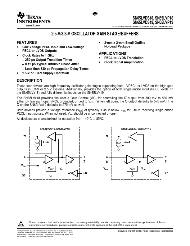
These four devices are high frequency oscillator gain stages supporting both LVPECL or LVDS on the high gain outputs in 3.3-V or 2.5-V systems. Additionally, provides the option of both single-ended input (PECL levels on the SN65LVx18) and fully differential inputs on the SN65LVx19. The SN65LVx18 provides the user a Gain Control (GC) for controlling the Q output from 300 m V to 860 m V either by leaving it open (NC), grounded, or tied to VCC. (When left open, the Q output defaults to 575 m V.) The Q on the SN65LVx19 defaults to 575 m V as well. Both devices provide a voltage reference (VBB) of typically 1.35 V below VCC for...