SN74AUP1G04
Description
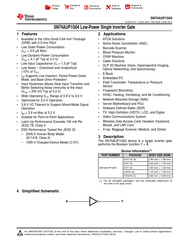
The SN74AUP1G04 device is a single inverter gate performs the Boolean function Y = A. Device Information(1) PART NUMBER PACKAGE BODY SIZE (NOM) SOT-23 (5) 2.90 mm × 1.60 mm SOT (5) 2.00 mm × 1.25 mm SN74AUP1G04 SOT (5) 1.60 mm × 1.20 mm USON (6) 1.45 mm × 1.00 mm X2SON (4) 0.80 mm × 0.80 mm (1) For all available packages, see the orderable addendum at the end of the data sheet.
Key Features
- 1 Available in the Ultra Small 0.64 mm2 Package (DPW) with 0.5-mm Pitch
- Low Static-Power Consumption (ICC = 0.9 μA Max)
- Low Dynamic-Power Consumption (Cpd = 4.1 pF Typ at 3.3 V)
- Low Input Capacitance (Ci = 1.5 pF Typ)
- Overshoot and Undershoot <10% of VCC
- Ioff Supports Live Insertion, Partial-Power-Down Mode, and Back-Drive Protection
- Input Hysteresis Allows Slow Input Transition and Better Switching Noise Immunity at the Input (Vhys = 250 mV Typ at 3.3 V)
- Wide Operating VCC Range of 0.8 V to 3.6 V
- Optimized for 3.3-V Operation
- 3.6-V I/O Tolerant to Support Mixed-Mode Signal Operation