SN74AUP1G08 Overview
Description
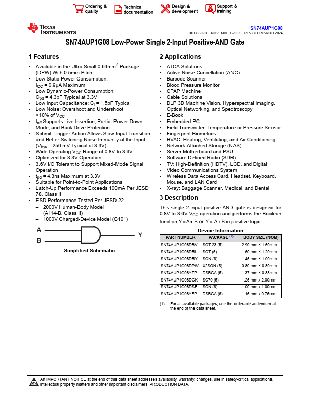
This single 2-input positive-AND gate is designed for 0.8V to 3.6V VCC operation and performs the Boolean function Y = A - B or Y = A +B in positive logic. Device Information PART NUMBER PACKAGE (1) BODY SIZE (NO.
Key Features
- Available in the Ultra Small 0.64mm2 Package (DPW) With 0.5mm Pitch
- Low Static-Power Consumption: ICC = 0.9μA Maximum
- Low Dynamic-Power Consumption: Cpd = 4.3pF Typical at 3.3V
- Low Input Capacitance: Ci = 1.5pF Typical
- Low Noise: Overshoot and Undershoot <10% of VCC
- Ioff Supports Live Insertion, Partial-Power-Down Mode, and Back Drive Protection
- Schmitt-Trigger Action Allows Slow Input Transition and Better Switching Noise Immunity at the Input (Vhys = 250 mV Typical at 3.3V)
- Wide Operating VCC Range of 0.8V to 3.6V
- Optimized for 3.3V Operation
- 3.6V I/O Tolerant to Support Mixed-Mode Signal Operation