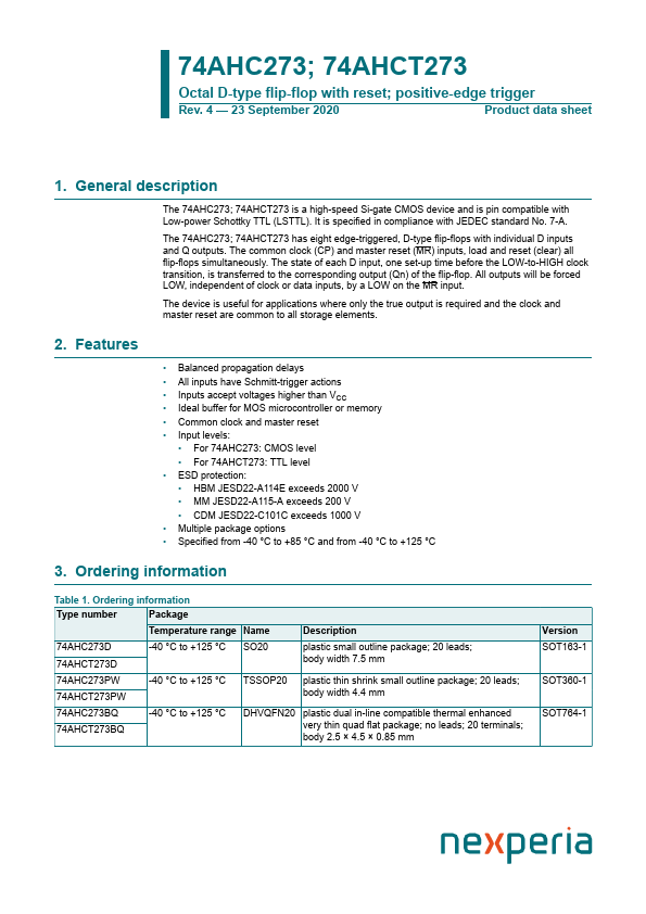
Datasheet4U Logo Datasheet4U.com

74AHC273 - Octal D-type flip-flop

Description

The 74AHC273; 74AHCT273 is a high-speed Si-gate CMOS device and is pin compatible with Low-power Schottky TTL (LSTTL).

It is specified in compliance with JEDEC standard No.

7-A.

Features

  • Balanced propagation delays.
  • All inputs have Schmitt-trigger actions.
  • Inputs accept voltages higher than VCC.
  • Ideal buffer for MOS microcontroller or memory.
  • Common clock and master reset.
  • Input levels:.
  • For 74AHC273: CMOS level.
  • For 74AHCT273: TTL level.
  • ESD protection:.
  • HBM JESD22-A114E exceeds 2000 V.
  • MM JESD22-A115-A exceeds 200 V.
  • CDM JESD22-C101C exceeds 1000 V.
  • Multiple p.

📥 Download Datasheet

Datasheet preview – 74AHC273

Datasheet Details

Part number 74AHC273
Manufacturer nexperia
File Size 265.73 KB
Description Octal D-type flip-flop
Datasheet download datasheet 74AHC273 Datasheet
Additional preview pages of the 74AHC273 datasheet.
Other Datasheets by nexperia

Full PDF Text Transcription

Click to expand full text
74AHC273; 74AHCT273 Octal D-type flip-flop with reset; positive-edge trigger Rev. 4 — 23 September 2020 Product data sheet 1. General description The 74AHC273; 74AHCT273 is a high-speed Si-gate CMOS device and is pin compatible with Low-power Schottky TTL (LSTTL). It is specified in compliance with JEDEC standard No. 7-A. The 74AHC273; 74AHCT273 has eight edge-triggered, D-type flip-flops with individual D inputs and Q outputs. The common clock (CP) and master reset (MR) inputs, load and reset (clear) all flip-flops simultaneously. The state of each D input, one set-up time before the LOW-to-HIGH clock transition, is transferred to the corresponding output (Qn) of the flip-flop. All outputs will be forced LOW, independent of clock or data inputs, by a LOW on the MR input.
Published: |