74LVC125A-Q100 Description
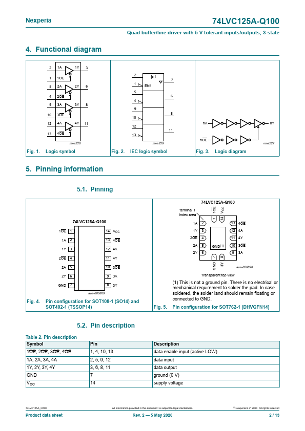
The 74LVC125A-Q100 consists of four non-inverting buffers/line drivers with 3-state outputs (nY) that are controlled by the output enable input (nOE). A HIGH at nOE causes the outputs to assume a high-impedance OFF-state. Inputs can be driven from either 3.3 V or 5 V devices.
74LVC125A-Q100 Key Features
- Automotive product qualification in accordance with AEC-Q100 (Grade 1)
- Specified from -40 °C to +85 °C and from -40 °C to +125 °C
- 5 V tolerant inputs/outputs for interfacing with 5 V logic
- Wide supply voltage range from 2.3 V to 3.6 V
- CMOS low power consumption
- Direct interface with TTL levels
- plies with JEDEC standard
- JESD8-7A (1.65 V to 1.95 V)
- JESD8-5A (2.3 V to 2.7 V)
- JESD8-C/JESD36 (2.7 V to 3.6 V)
74LVC125A-Q100 Applications
- Automotive product qualification in accordance with AEC-Q100 (Grade 1)
- Specified from -40 °C to +85 °C and from -40 °C to +125 °C
- 5 V tolerant inputs/outputs for interfacing with 5 V logic
- Wide supply voltage range from 2.3 V to 3.6 V