74LVC2G34-Q100 Description
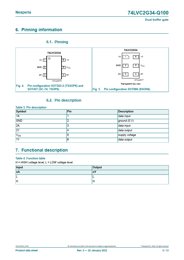
The 74LVC2G34-Q100 is a dual buffer. Inputs can be driven from either 3.3 V or 5 V devices.
74LVC2G34-Q100 Key Features
- Automotive product qualification in accordance with AEC-Q100 (Grade 1)
- Specified from -40 °C to +85 °C and -40 °C to +125 °C
- Wide supply voltage range from 1.65 V to 5.5 V
- Overvoltage tolerant inputs to 5.5 V
- High noise immunity
- ±24 mA output drive (VCC = 3.0 V)
- CMOS low power dissipation
- IOFF provides partial Power-down mode operation
- Direct interface with TTL levels
- Latch-up performance exceeds 250 mA
74LVC2G34-Q100 Applications
- Automotive product qualification in accordance with AEC-Q100 (Grade 1)
- Specified from -40 °C to +85 °C and -40 °C to +125 °C
- Wide supply voltage range from 1.65 V to 5.5 V
- Overvoltage tolerant inputs to 5.5 V