Datasheet Details
| Part number | CY2SSTV850 |
|---|---|
| Manufacturer | Cypress Semiconductor |
| File Size | 152.68 KB |
| Description | Differential Clock Buffer/Driver |
| Datasheet |
 CY2SSTV850_CypressSemiconductor.pdf CY2SSTV850_CypressSemiconductor.pdf
|
| Part number | CY2SSTV850 |
|---|---|
| Manufacturer | Cypress Semiconductor |
| File Size | 152.68 KB |
| Description | Differential Clock Buffer/Driver |
| Datasheet |
CY2SSTV850_CypressSemiconductor.pdf
|
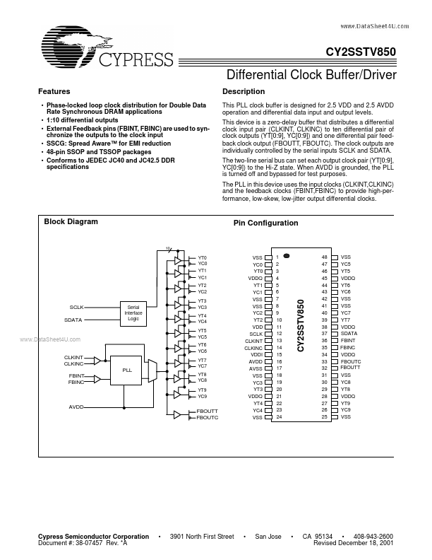
This PLL clock buffer is designed for 2.5 VDD and 2.5 AVDD operation and differential data input and output levels.
📁 CY2SSTV850 Similar Datasheet