Description
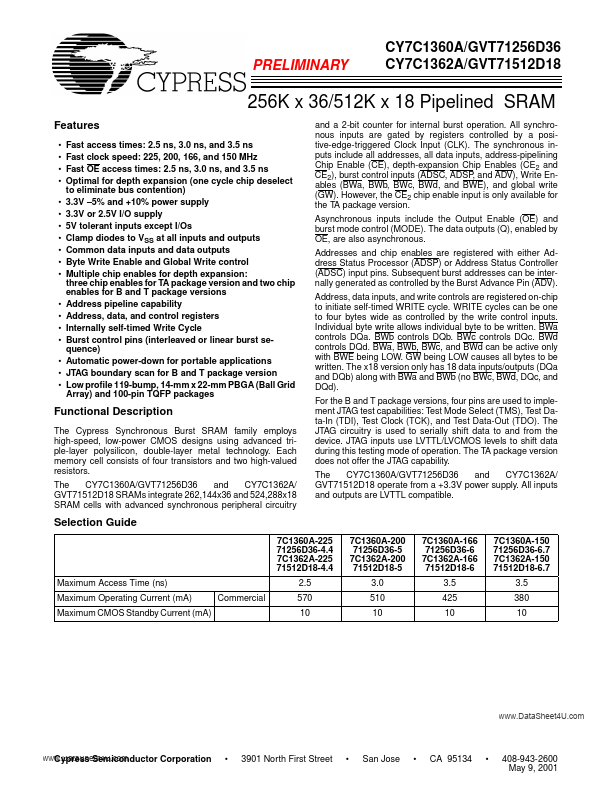
( DataSheet : www.DataSheet4U.com ) 1CY7C1329 PRELIMINARY CY7C1360A/GVT71256D36 CY7C1362A/GVT71512D18 256K x 36/512K x 18 Pipelined SRAM .
The Cypress Synchronous Burst SRAM family employs high-speed, low-power CMOS designs using advanced triple-layer polysilicon, double-layer metal techn.
Features
* Fast access times: 2.5 ns, 3.0 ns, and 3.5 ns Fast clock speed: 225, 200, 166, and 150 MHz Fast OE access times: 2.5 ns,
Applications
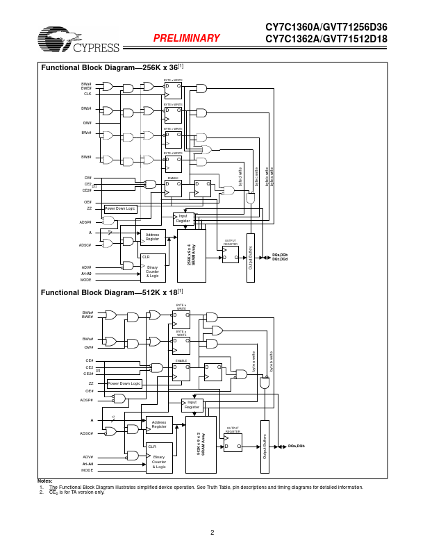
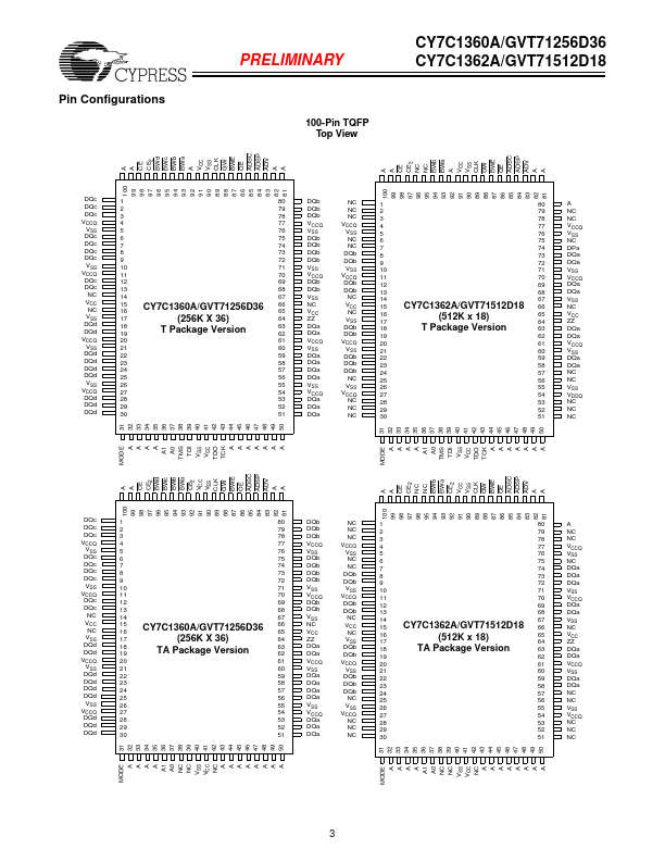
* JTAG boundary scan for B and T package version Low profile 119-bump, 14-mm x 22-mm PBGA (Ball Grid Array) and 100-pin TQFP packages and a 2-bit counter for internal burst operation. All synchronous inputs are gated by registers controlled by a positive-edge-triggered Clock Input (CLK). The synchrono