Description
SYMBOL CS0_n, CS1_n
CK_c, CK_t CKE0, CKE1 CA0 ~ CA9 DQ0 ~ DQ31 DM0 ~ DM3 DQS0_t ~ DQS3_t DQS0_c ~ DQS3_c
ZQ VDD1 VDD2 VSS VDDQ VDDCA VSSCA VSSQ VREF ODT
8Gb,16Gb: 178-Ball, LPDDR3 SDRAM
DESCRIPTION Chip Select
Differential Clocks Clock Enable
Command / Address Data I/O
Input Data Mask Differential Data Strobe (rising edge) Differential Data Strobe (falling edge)
Drive Strength Calibration Core Power Supply Core Power Supply Ground I/O Power Supply CA Power Supply CA Ground I/O Ground Reference
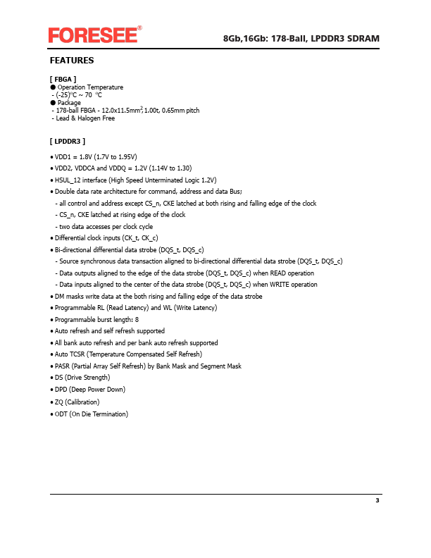
Features
- [ FBGA ].
- Operation Temperature - (-25)oC ~ 70 oC.
- Package - 178-ball FBGA - 12.0x11.5mm2, 1.00t, 0.65mm pitch - Lead & Halogen Free
8Gb,16Gb: 178-Ball, LPDDR3 SDRAM
[ LPDDR3 ].
- VDD1 = 1.8V (1.7V to 1.95V).
- VDD2, VDDCA and VDDQ = 1.2V (1.14V to 1.30).
- HSUL_12 interface (High Speed Unterminated Logic 1.2V).
- Double data rate architecture for command, address and data Bus;
- all control and address except CS_n, CKE latched at both rising and falling edge of the clock.


