Datasheet Details
| Part number | 4050B |
|---|---|
| Manufacturer | Fairchild Semiconductor |
| File Size | 63.51 KB |
| Description | Hex Inverting Buffer / Hex Non-Inverting Buffer |
| Datasheet |
 4050B Datasheet 4050B Datasheet
|
|
|
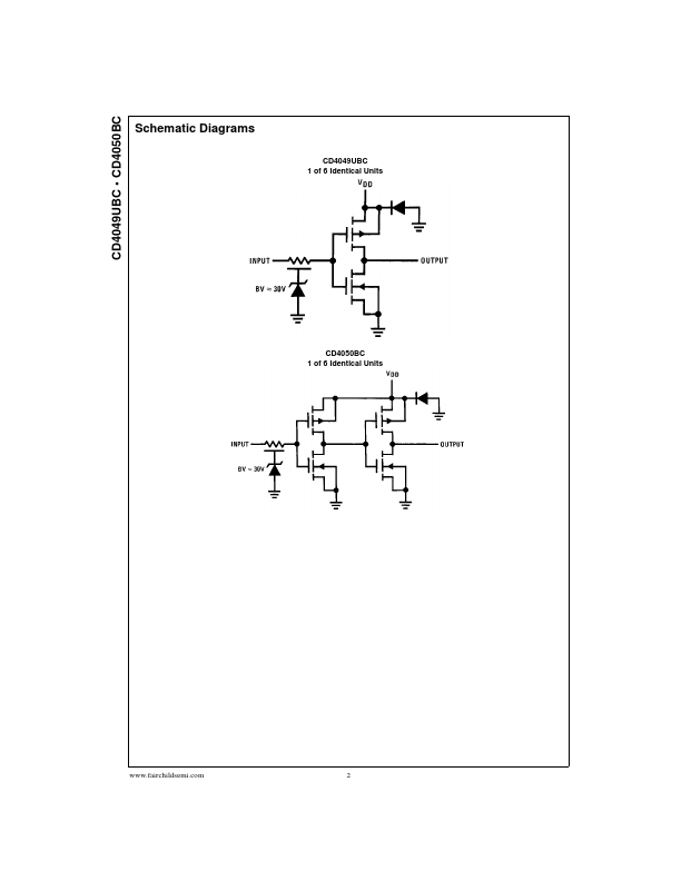
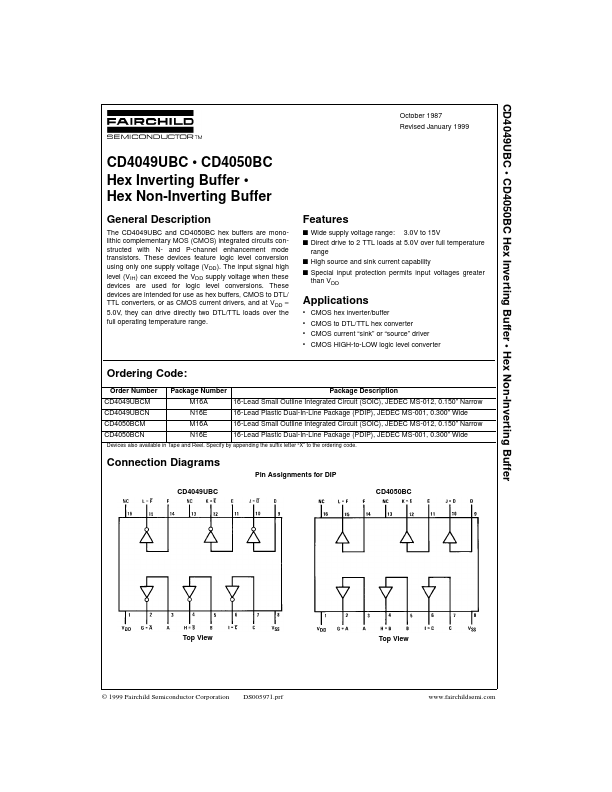
The CD4049UBC and CD4050BC hex buffers are monolithic complementary MOS (CMOS) integrated circuits constructed with N- and P-channel enhancement mode transistors.
These devices feature logic level conversion using only one supply voltage (VDD ).
| Part number | 4050B |
|---|---|
| Manufacturer | Fairchild Semiconductor |
| File Size | 63.51 KB |
| Description | Hex Inverting Buffer / Hex Non-Inverting Buffer |
| Datasheet |
4050B Datasheet
|
|
|
|