FDB6035L Overview
Key Specifications
Max Operating Temp: 175 °C
Min Operating Temp: -65 °C
Description
These N-Channel logic level enhancement mode power field effect transistors are produced using Fairchild's proprietary, high cell density, DMOS technology. This very high density process is especially tailored to minimize on-state resistance.
Key Features
- RDS(ON) = 0.011 Ω @ VGS=10 V RDS(ON) = 0.019 Ω @ VGS=4.5 V
- Low gate charge (typical 34 nC)
- Low Crss (typical 175 pF)
- Fast switching speed
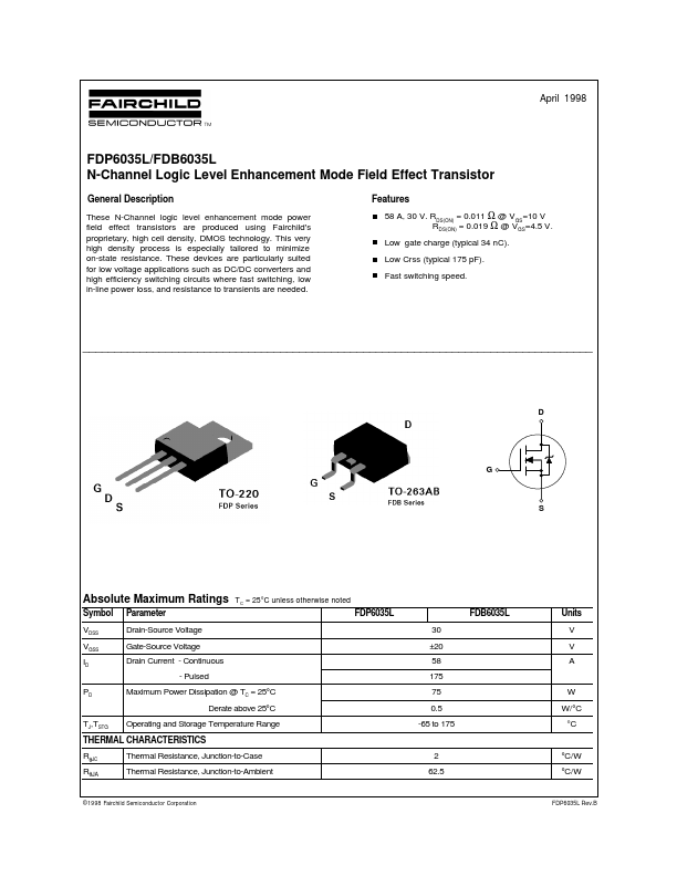
- ________________________________________________________________________________ D G S