Description
Drain-Source Voltage Continuous Drain Current Pulsed Drain Current Gate-Source Voltage Repetitive and Non-Repetitive Maximum Avalanche Current Non-Repetitive Maximum Avalanche Energy Repetitive Maximum Avalanche Energy Peak Diode Recovery dV/dt Peak Diode Recovery -di/dt Maximum Power Dissipation Operating and Storage Temperature range Symbol VDS VDSX ID I DP VGS I AR E AS E AR dV/dt -di/dt PD Tch Tstg Characteristics 500 500 ±23 ±92 ±30 23 767.3 31.5 9.3 100 2.50 315 150 -55 to + 150 Unit V V A
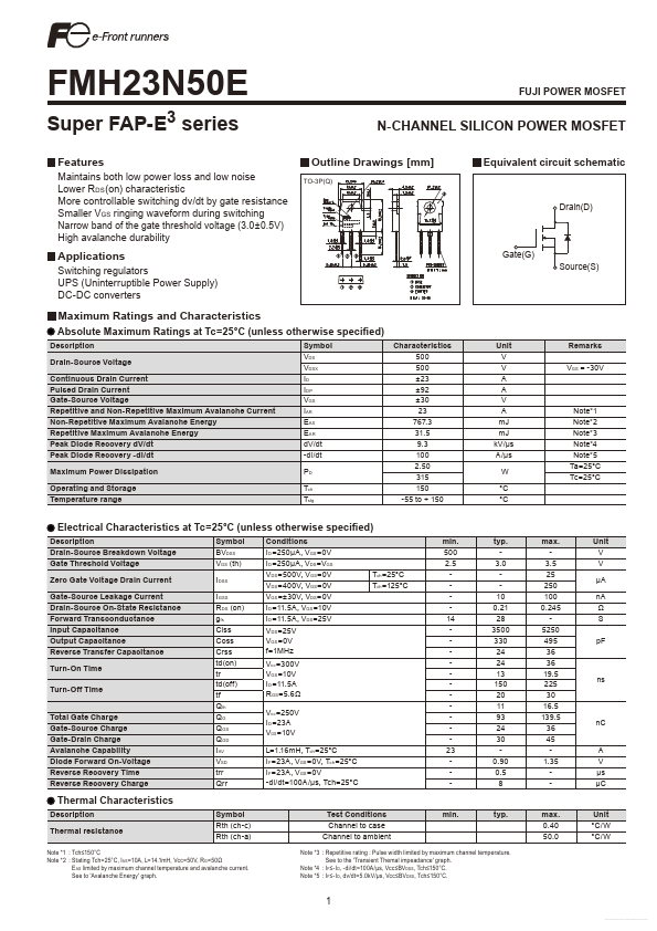
Features
- Maintains both low power loss and low noise Lower RDS (on) characteristic More controllable switching dv/dt by gate resistance Smaller VGS ringing waveform during switching Narrow band of the gate threshold voltage (3.0±0.5V) High avalanche durability
FUJI POWER MOSFET
N-.
 23N50E-FujiElectric.pdf