Description
Table
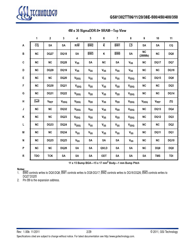
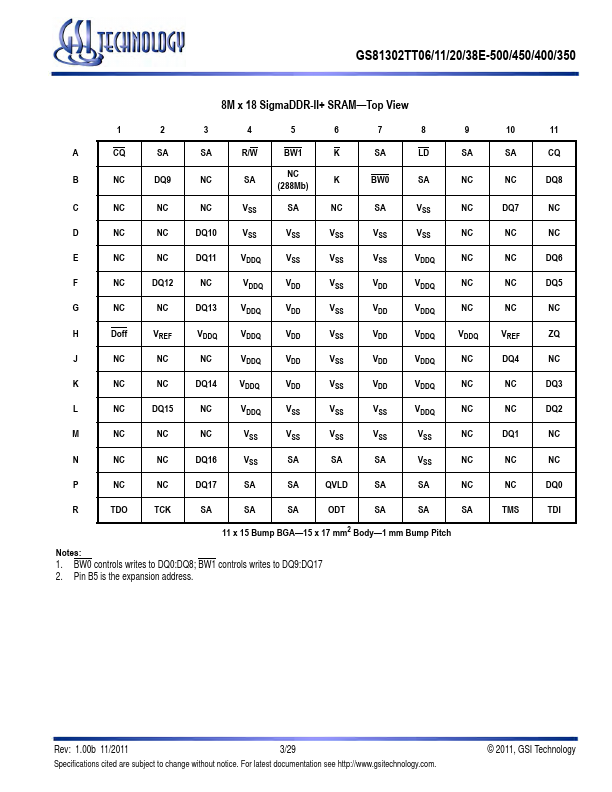
Symbol
Description
Type Comments
SA
Synchronous Address Inputs
Input
R/W
Synchronous Read/Write
Input
High: Read Low: Write
BW0
BW3
Synchronous Byte Writes
Input Active Low
LD
Synchronous Load Pin
Input Active Low
K
Input Clock
Input Active High
K
Input Clock
Input Active Low
TMS
Test Mode Select
Input
TDI
Test Data Input
Input
TCK
Test Clock Input
Input
TDO
Test Data Output
Output
VREF
HSTL Inpu
Features
- 2.5 Clock Latency.
- Simultaneous Read and Write SigmaDDRTM Interface.
- JEDEC-standard pinout and package.
- Double Data Rate interface.
- Byte Write controls sampled at data-in time.
- Burst of 2 Read and Write.
- Dual-Range On-Die Termination (ODT) on Data (D), Byte
Write (BW), and Clock (K, K) inputs.
- 1.8 V +100/.
- 100 mV core power supply.
- 1.5 V or 1.8 V HSTL Interface.
- Pipelined read operation.
- Fu.
 GS81302TT06E-500-GSITechnology.pdf